LT1576/LT1576-5
U
W U U
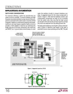
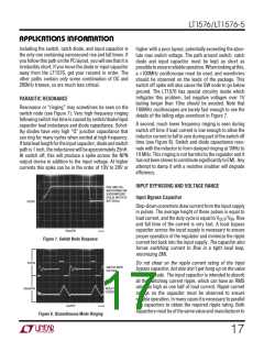
APPLICATIONS INFORMATION
At power-up, when VC is being clamped by the FB pin (see
Figure2,Q2),thesyncfunctionisdisabled.Thisallowsthe
frequency foldback to operate in the shorted output con-
dition. During normal operation, switching frequency is
controlledbytheinternaloscillatoruntiltheFBpinreaches
0.7V, after which the SYNC pin becomes operational. If no
synchronization is required, this pin should be connected
to ground.
2
0.2 1 5
(
)( ) ( )
−9
3
P
=
+ 60• 10
1 10 200• 10
( )( )
SW
10
= 0.1 + 0.12 = 0.22W
2
5 1/50
( ) (
)
P
=
= 0.05W
BOOST
10
2
5 0.004
( ) (
)
−3
−3
P =10 0.55• 10
+5 1.6• 10
+
Q
THERMAL CALCULATIONS
10
= 0.02W
Power dissipation in the LT1576 chip comes from four
sources: switch DC loss, switch AC loss, boost circuit
current,andinputquiescentcurrent.Thefollowingformu-
las show how to calculate each of these losses. These
formulas assume continuous mode operation, so they
should not be used for calculating efficiency at light load
currents.
Total power dissipation is 0.22 + 0.05 + 0.02 = 0.29W.
Thermal resistance for LT1576 package is influenced by
the presence of internal or backside planes. With a full
plane under the SO package, thermal resistance will be
about 80°C/W. No plane will increase resistance to about
120°C/W. To calculate die temperature, add in worst-case
ambient temperature:
Switch loss:
2
R
I
V
OUT
(
) (
)
SW OUT
TJ = TA + θJA (PTOT
)
P
=
+ 60ns I
V
f
(
)( )( )
SW
OUT IN
V
IN
With the SO-8 package (θJA = 80°C/W), at an ambient
temperature of 50°C,
Boost current loss:
TJ = 50 + 80 (0.29) = 73.2°C
2
V
I
/50
(
)
OUT OUT
Die temperature is highest at low input voltage, so use
lowest continuous input operating voltage for thermal
calculations.
P
=
BOOST
V
IN
Quiescent current loss:
FREQUENCY COMPENSATION
−3
−3
P = V 0.55• 10
+ V
1.6• 10
Q
IN
OUT
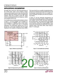
Loop frequency compensation of switching regulators
can be a rather complicated problem because the reactive
components used to achieve high efficiency also intro-
duce multiple poles into the feedback loop. The inductor
and output capacitor on a conventional step-down con-
verter actually form a resonant tank circuit that can exhibit
peaking and a rapid 180° phase shift at the resonant
frequency. Bycontrast, theLT1576usesa“currentmode”
architecture to help alleviate phase shift created by the
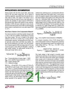
inductor. The basic connections are shown in Figure 9.
Figure 10 shows a Bode plot of the phase and gain of the
power section of the LT1576, measured from the VC pin to
2
V
0.004
(
)
OUT
+
V
IN
RSW = Switch resistance (≈0.2Ω)
60ns = Equivalent switch current/voltage overlap time
f = Switch frequency
Example: with VIN = 10V, VOUT = 5V and IOUT = 1A:
19

 Linear [ Linear ]