LT1576/LT1576-5
U
W U U
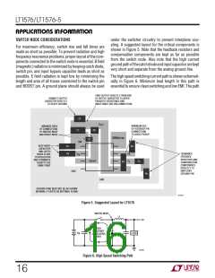
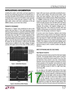
APPLICATIONS INFORMATION
including the switch, catch diode, and input capacitor is
the only one containing nanosecond rise and fall times. If
you follow this path on the PC layout, you will see that it is
irreducibly short. If you move the diode or input capacitor
away from the LT1576, get your resumé in order. The
other paths contain only some combination of DC and
200kHz triwave, so are much less critical.
higher with a poor layout, potentially exceeding the abso-
lute max switch voltage. The path around switch, catch
diode and input capacitor must be kept as short as
possibletoensurereliableoperation.Whenlookingatthis,
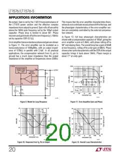
a >100MHz oscilloscope must be used, and waveforms
should be observed on the leads of the package. This
switch off spike will also cause the SW node to go below
ground. The LT1576 has special circuitry inside which
mitigates this problem, but negative voltages over 1V
lasting longer than 10ns should be avoided. Note that
100MHz oscilloscopes are barely fast enough to see the
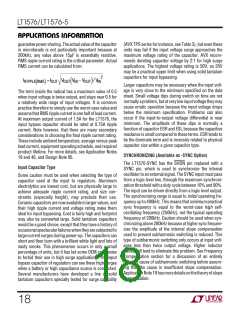
details of the falling edge overshoot in Figure 7.
PARASITIC RESONANCE
Resonance or “ringing” may sometimes be seen on the
switch node (see Figure 7). Very high frequency ringing
following switch rise time is caused by switch/diode/input
capacitor lead inductance and diode capacitance. Schot-
tky diodes have very high “Q” junction capacitance that
can ring for many cycles when excited at high frequency.
Iftotalleadlengthfortheinputcapacitor, diodeandswitch
path is 1 inch, the inductance will be approximately 25nH.
At switch off, this will produce a spike across the NPN
output device in addition to the input voltage. At higher
currents this spike can be in the order of 10V to 20V or
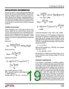
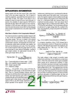
A second, much lower frequency ringing is seen during
switch off time if load current is low enough to allow the
inductor current to fall to zero during part of the switch off
time (see Figure 8). Switch and diode capacitance reso-
nate with the inductor to form damped ringing at 1MHz to
10 MHz. This ringing is not harmful to the regulator and it
hasnotbeenshowntocontributesignificantlytoEMI. Any
attempt to damp it with a resistive snubber will degrade
efficiency.
INPUT BYPASSING AND VOLTAGE RANGE
Input Bypass Capacitor
RISE AND FALL
WAVEFORMS ARE
SUPERIMPOSED
(PULSE WIDTH IS
NOT 350ns)
5V/DIV
Step-down converters draw current from the input supply
in pulses. The average height of these pulses is equal to
load current, and the duty cycle is equal to VOUT/VIN. Rise
and fall time of the current is very fast. A local bypass
capacitor across the input supply is necessary to ensure
proper operation of the regulator and minimize the ripple
current fed back into the input supply. The capacitor also
forces switching current to flow in a tight local loop,
minimizing EMI.
50ns/DIV
1374 F07
Figure 7. Switch Node Response
5V/DIV
Do not cheat on the ripple current rating of the Input
bypass capacitor, but also don’t get hung up on the value
in microfarads. The input capacitor is intended to absorb
all the switching current ripple, which can have an RMS
value as high as one half of load current. Ripple current
ratings on the capacitor must be observed to ensure
reliable operation. In many cases it is necessary to parallel
two capacitors to obtain the required ripple rating. Both
capacitors must be of the same value and manufacturer to
SWITCH NODE
VOLTAGE
50mA/DIV
INDUCTOR
CURRENT
1µs/DIV
1374 F08
Figure 8. Discontinuous Mode Ringing
17

 Linear [ Linear ]