LT1576/LT1576-5
U
W U U
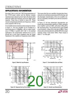
APPLICATIONS INFORMATION
SWITCH NODE CONSIDERATIONS
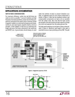
under the switcher circuitry to prevent interplane cou-
pling. A suggested layout for the critical components is
shown in Figure 5. Note that the feedback resistors and
compensation components are kept as far as possible
from the switch node. Also note that the high current
groundpathofthecatchdiodeandinputcapacitorarekept
very short and separate from the analog ground line.
For maximum efficiency, switch rise and fall times are
made as short as possible. To prevent radiation and high
frequency resonance problems, proper layout of the com-
ponents connected to the switch node is essential. B field
(magnetic) radiation is minimized by keeping catch diode,
switch pin, and input bypass capacitor leads as short as
possible. E field radiation is kept low by minimizing the
length and area of all traces connected to the switch pin
and BOOST pin. A ground plane should always be used
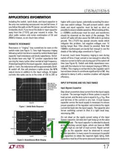
Thehighspeedswitchingcurrentpathisshownschemati-
cally in Figure 6. Minimum lead length in this path is
essential to ensure clean switching and low EMI. The path
TAKE OUTPUT DIRECTLY FROM END
CONNECT OUTPUT
CAPACITOR DIRECTLY
TO HEAVY GROUND
OF OUTPUT CAPACITOR TO AVOID
PARASITIC RESISTANCE AND
INDUCTANCE (KELVIN CONNECTION)
C1
V
OUT
MINIMUM SIZE
OF FEEDBACK PIN
CONNECTIONS
MINIMIZE AREA
OF CONNECTIONS
TO SWITCH NODE
AND BOOST NODE
L1
D2
TO AVOID PICKUP
SHDN/SYNC
C2
SW
IN
KEEP INPUT
CAPACITOR
AND CATCH
R2
D1
C3
TERMINATE
V
FB
DIODE CLOSE
TO REGULATOR
AND TERMINATE
THEM TO THE
SAME POINT
FEEDBACK
RESISTORS AND
COMPENSATION
COMPONENTS
DIRECTLY TO
SWITCHER
C
BOOST
V
C
C
R1
GND
R
GROUND PIN
C
GND
GROUND RING NEED NOT BE AS SHOWN
(NORMALLY EXISTS AS INTERNAL PLANE)
1576 F05
Figure 5. Suggested Layout for LT1576
SWITCH NODE
L1
5V
HIGH
FREQUENCY
CIRCULATING
PATH
V
IN
LOAD
1576 F06
Figure 6. High Speed Switching Path
16

 Linear [ Linear ]