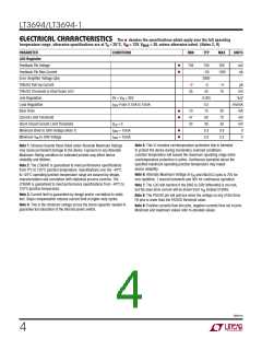
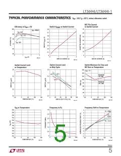
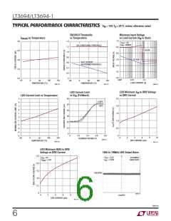
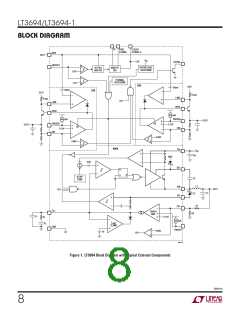
LT3694/LT3694-1
PIN FUNCTIONS (FE/UFD)
V (Pin 1/Pins 27, 28): The V pin supplies power to the
for the LDO regulators. The DRV pins can provide up to
6V of base drive.
IN
IN
internal switch of the 2.6A regulator and to the LT3694’s
internal reference and start-up circuitry. This pin must be
locally bypassed.
LIM2,LIM3(Pins10,11/Pins9,14):TheLIMpinsprovide
current limiting on the LDO pass transistors by sensing
a voltage on an external sense resistor connected to the
BIAS pin. These pins should be connected to BIAS if this
function is not used.
EN/UVLO (Pin 2/Pin 1): The EN/UVLO pin is used to shut
down the LT3694. It can be driven from a logic level or
used as an undervoltage lockout by connecting a resistor
divider from V .
IN
GND (Pins 10, 11, 12, 13, 25, 26) UFD Package Only:
Power and Signal Ground.
CLKOUT (Pin 3/Pin 2): Digital Clock Output. The CLKOUT
pin allows synchronization of other switching regulators
(LT3694-1 only).
V
(Pin 16/Pin 19): Output of the Internal Error Amp.
C1
The voltage on this pin controls the peak switch cur-
rent. This pin is normally used to compensate the
control loop. The switching regulator can be shut
SYNC (Pin 3/Pin 2): Frequency Synchronization Input.
Connectafrequencysourcetothisinputifsynchronization
is desired. Connect SYNC to ground if not used (LT3694
only).
down by pulling the V pin to ground with an NMOS
C1
or NPN transistor.
PGOOD (Pin 4/Pin 3): Open Collector Output. PGOOD is
BIAS (Pin 17/Pin 20): The BIAS pin supplies the current
to the LT3694’s internal regulator and boost circuits. This
must be connected to a voltage source above 3V, usually
pulled low when any of the three regulators drops out of
regulation (V < 90% of nominal value).
FB
to V
. The LDO pass transistor base current will also
OUT1
RT (Pin 5/Pin 4): The RT pin requires a resistor to ground
tosettheoperatingfrequencyoftheLT3694.Ifsynchroniz-
ing the LT3694 to an external clock, the resistor should
be set to program the frequency at least 20% below the
synchronization frequency.
come from the BIAS pin if it is at least 1.8V above the
LDO output.
BST (Pin 18/Pin 21): The BST pin is used to provide a
drive voltage, higher than the input voltage, to the internal
bipolar NPN power switch.
TRK/SS1, TRK/SS2 , TRK/SS3 (Pins 6, 7, 14/Pins 5, 6, 17):
The TRK/SS pins allow a regulator to track the output of
another regulator. When the TRK/SS pin is below 0.75V,
the FB pin regulates to the TRK/SS voltage. This pin can
also beusedasasoft-startbyconnectingacapacitorfrom
TRK/SS to ground. The TRK/SS pins should be left open
if neither feature is used.
DA (Pin 19/Pin 22): The DA pin senses the catch diode
current to prevent excessive inductor current in output
overload or short-circuit conditions.
SW (Pin 20/Pins 23, 24): Output of the Internal Power
Switch. Connect this pin to the inductor and switching
diode.
FB1, FB2, FB3 (Pins 15, 8, 13/Pins 18, 7, 16): Negative
Inputs of the Error Amplifiers. The LT3694 regulates each
feedback pin to the lesser of 0.75V or the corresponding
TRK/SS pin voltage. Connect the feedback resistor divider
taps to these pins.
Exposed Pad (Pin 21/Pin 29): Ground. The underside
exposed pad metal of the package provides both electrical
contact to ground and a conductive thermal path to the
printedcircuitboard.TheExposedPadmustbesolderedto
a grounded pad on the circuit board for proper operation.
DRV2, DRV3 (Pins 9, 12/Pins 8, 15): The DRV pins
provide the base drive for the external NPN transistors
36941fb
7

 Linear [ Linear ]