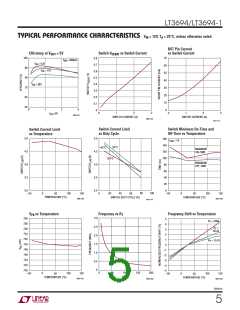
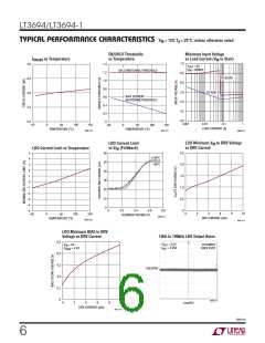
LT3694/LT3694-1
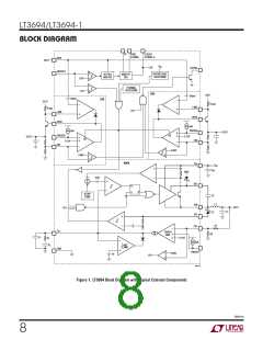
OPERATION
Unless specifically noted, this data sheet refers to both the
LT3694 and the LT3694-1 generically as the LT3694.
thecurrentthroughtheinductortotheoutput. Theinternal
error amplifier regulates the output voltage by continually
adjusting the V pin voltage. The threshold for switching
C1
The LT3694 is a constant-frequency, current mode, buck
regulator with an internal power switch plus two low
dropout linear regulator controllers. The three regulators
share common circuitry including input source, voltage
reference, undervoltage lockout, and enable, but are oth-
erwise independent. Operation can be best understood by
referring to the Block Diagram (Figure 1).
on the V pin is 0.75V and an active clamp of 2V limits
C1
the output current.
Overcurrent protection is provided by the DA comparator.
The DA comparator senses the catch diode current and
will delay the switch-on cycle if the diode current is too
high at the beginning of a cycle.
If the EN/UVLO pin is below 0.35V (min), the LT3694 is
shut down and draws <2µA from the input source tied to
IN1
The TRK/SS pins override the 0.75V reference for the FB
pins when the TRK/SS pins are below 0.75V. This allows
eithercoincidentorratiometricsupplytrackingonstart-up
as well as a soft-start capability.
V
. If the EN/UVLO pin is driven above 0.5V (typ), the
internalbiascircuitsturnon,includingtheinternalregulator,
reference and master oscillator. The switching regulator
will only begin to operate when the EN/UVLO pin reaches
>1.20V (typ). The EN/UVLO pin can be driven from a logic
gate or can be used as an undervoltage lockout by using
The switch driver operates either from V or from the BST
IN
pin. An external capacitor is used to generate a voltage at
the BST pin that is higher than the input supply. This al-
lows the driver to saturate the internal bipolar NPN power
switch for efficient operation.
a resistor divider to V .
IN
Theswitcherisacurrentmoderegulator.Insteadofdirectly
modulatingthedutycycleofthepowerswitch,thefeedback
loop controls the peak current in the switch during each
cycle. Compared to voltage mode control, current mode
control improves loop dynamics and provides cycle-by-
cycle current limit.
The BIAS pin allows the internal circuitry to draw its cur-
rent from a voltage supply lower than V , reducing power
IN
dissipation and increasing efficiency. If the voltage on the
BIAS pin falls below 2.7V, then its quiescent current will
flow from V .
IN
TheLDOregulatorusesanexternalNPNpasstransistorto
form a linear regulator. The loop is internally compensated
tobestablewithaminimumloadcapacitanceof2.2µF.The
LDOalsohasafoldbackcurrentlimiteravailabletoprotect
the external transistor under overload conditions
A pulse from the oscillator sets the RS flip-flop and turns
on the internal NPN bipolar power switch. Current in the
switch and the external inductor begins to increase. When
this current exceeds a level determined by the voltage
at V , the current comparator resets the RS flip-flop,
C1
turning off the switch. The current in the inductor flows
through the external, Schottky, catch diode, and begins to
decrease.Thecyclebeginsagainatthenextpulsefromthe
The overvoltage detection shuts down the LT3694 if the
input voltage goes above 38V. This will prevent the switch
from turning on under high voltage conditions and allows
the LT3694 to survive transient input voltages up to 70V.
oscillator. In this way, the voltage on the V pin controls
C1
36941fb
9

 Linear [ Linear ]