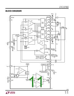
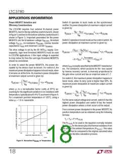
LTC3780
OPERATION
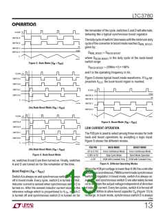
on. switch A and synchronous switch B are alternately
turned on to maintain the output voltage independent of
direction of inductor current. Every ten cycles, synchro-
controller will enter continuous current buck mode for
one cycle to discharge inductor current. In the following
cycle, thecontrollerwillresumeDCMboostoperation. For
buckoperation,constantfrequencydiscontinuouscurrent
mode sets a minimum negative inductor current level.
synchronous switch B is turned off whenever inductor
current is lower than this level. At very light loads, this
constant frequency operation is not as efficient as Burst
Mode operation or skip-cycle, but does provide lower
noise, constant frequency operation.
nous switch D is forced off for about 300ns to allow C
B
to recharge. This is the least efficient operating mode at
light load, but may be desirable in certain applications. In
this mode, the output can source or sink current.
WhentheFCBpinvoltageisbelowV
–1V,butgreater
INTVCC
than 0.8V, the controller enters Burst Mode operation in
boost operation or enters skip-cycle mode in buck opera-
tion. During boost operation, Burst Mode operation sets a
minimum output current level before inhibiting the switch
C and turns off synchronous switch D when the inductor
current goes negative. This combination of requirements
FREQUENCY SYNCHRONIZATION AND
FREQUENCY SETUP
The phase-locked loop allows the internal oscillator to be
synchronized to an external source via the PLLIN pin. The
phase detector output at the PLLFLTR pin is also the DC
frequency control input of the oscillator. The frequency
ranges from 200kHz to 400kHz, corresponding to a DC
voltage input from 0V to 2.4V at PLLFLTR. When locked,
the PLL aligns the turn on of the top MOSFET to the ris-
ing edge of the synchronizing signal. When PLLIN is left
open, the PLLFLTR pin goes low, forcing the oscillator to
its minimum frequency.
will, at low currents, force the I pin below a voltage
TH
threshold that will temporarily inhibit turn-on of power
switches C and D until the output voltage drops. There is
100mV of hysteresis in the burst comparator tied to the
I
TH
pin. This hysteresis produces output signals to the
MOSFETs C and D that turn them on for several cycles,
followed by a variable “sleep” interval depending upon the
loadcurrent.Themaximumoutputvoltagerippleislimited
to 3% of the nominal DC output voltage as determined
by a resistive feedback divider. During buck operation at
no load, switch A is turned on for its minimum on-time.
This will not occur every clock cycle when the output load
current drops below 1% of the maximum designed load.
The body diode of synchronous switch B or the Schottky
diode, which is in parallel with switch B, is used to dis-
charge the inductor current; switch B only turns on every
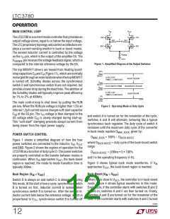
INTV /EXTV Power
CC
CC
Power for all power MOSFET drivers and most inter-
nal circuitry is derived from the INTV pin. When the
CC
EXTV pin is left open, an internal 6V low dropout linear
CC
regulator supplies INTV power. If EXTV is taken above
CC
CC
5.7V, the 6V regulator is turned off and an internal switch
ten clock cycles to allow C to recharge. As load current
B
is turned on, connecting EXTV to INTV . This allows
CC
CC
is applied, switch A turns on every cycle, and its on-time
begins to increase. At higher current, switch B turns on
briefly after each turn-off of switch A. switches C and D
remain off at light load, except to refresh CA (Figure 11)
every 10 clock cycles. In Burst Mode operation/skip-cycle
mode, the output is prevented from sinking current.
the INTV power to be derived from a high efficiency
CC
external source.
POWER GOOD (PGOOD) PIN
ThePGOODpinisconnectedtoanopendrainofaninternal
MOSFET. TheMOSFETturnsonandpullsthepinlowwhen
the output is not within 7.5% of the nominal output level
as determined by the resistive feedback divider. When
the output meets the 7.5% requirement, the MOSFET
is turned off and the pin is allowed to be pulled up by an
external resistor to a source of up to 7V.
When the FCB pin voltage is tied to the INTV pin, the
CC
controllerentersconstantfrequencydiscontinuouscurrent
mode (DCM). For boost operation, synchronous switch D
is held off whenever the I pin is below a threshold volt-
TH
age. In every cycle, switch C is used to charge inductor
current. After the output voltage is high enough, the
3780fe
14

 Linear Systems [ Linear Systems ]