LTC3780
APPLICATIONS INFORMATION
Power MOSFET Selection and
Efficiency Considerations
Switch B operates in buck mode as the synchronous
rectifier. Its power dissipation at maximum output current
is given by:
The LTC3780 requires four external N-channel power
MOSFETs,twoforthetopswitches(switchAandD,shown
inFigure1)andtwoforthebottomswitches(switchBand C
shown in Figure 1). Important parameters for the power
V – VOUT
IN
P
=
sIOUT(MAX)2 s ρT sRDS(ON)
B,BUCK
V
IN
Switch C operates in boost mode as the control switch. Its
power dissipation at maximum current is given by:
MOSFETs are the breakdown voltage V
, threshold
BR,DSS
, reverse transfer
voltage V
, on-resistance R
GS,TH
DS(ON)
and maximum current I
capacitance C
.
RSS
DS(MAX)
The drive voltage is set by the 6V INTV supply. Con-
V
– V V
IN OUT
CC
(
)
OUT
PC,BOOST
=
sIOUT(MAX)2 s ρT sRDS(ON)
sequently, logic-level threshold MOSFETs must be used
in LTC3780 applications. If the input voltage is expected
to drop below 5V, then the sub-logic threshold MOSFETs
should be considered.
2
V
IN
IOUT(MAX)
+ k s VOUT3 s
sCRSS s f
V
IN
In order to select the power MOSFETs, the power dis-
sipated by the device must be known. For switch A, the
maximumpowerdissipationhappensinboostmode,when
it remains on all the time. Its maximum power dissipation
at maximum output current is given by:
whereC isusuallyspecifiedbytheMOSFETmanufactur-
RSS
ers. The constant k, which accounts for the loss caused
by reverse recovery current, is inversely proportional to
the gate drive current and has an empirical value of 1.7.
For switch D, the maximum power dissipation happens in
boost mode, when its duty cycle is higher than 50%. Its
maximum power dissipation at maximum output current
is given by:
2
⎛ VOUT
⎞
⎠
PA,BOOST
=
sIOUT(MAX) s ρT sRDS(ON)
⎜
⎟
⎝ V
IN
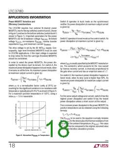
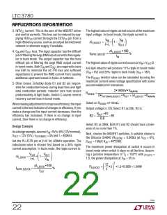
where ρ is a normalization factor (unity at 25°C) ac-
T
2
⎛
⎞
⎟
⎠
VOUT
V
VOUT
counting for the significant variation in on-resistance with
temperature,typicallyabout0.4%/°CasshowninFigure 9.
For a maximum junction temperature of 125°C, using a
IN
PD,BOOST
=
s
sIOUT(MAX) sρT sRDS(ON)
⎜
V
⎝
IN
For the same output voltage and current, switch A has the
highest power dissipation and switch B has the lowest
power dissipation unless a short occurs at the output.
value ρ = 1.5 is reasonable.
T
2.0
1.5
1.0
0.5
0
From a known power dissipated in the power MOSFET, its
junction temperature can be obtained using the following
formula:
T = T + P • R
J
A
TH(JA)
The R
to be used in the equation normally includes
TH(JA)
the R
for the device plus the thermal resistance from
TH(JC)
the case to the ambient temperature (R
). This value
TH(JC)
of T can then be compared to the original, assumed value
J
50
100
–50
150
0
used in the iterative calculation process.
JUNCTION TEMPERATURE (°C)
3780 F09
Figure 9. Normalized RDS(ON) vs Temperature
3780fe
18

 Linear Systems [ Linear Systems ]