LTC3780
PIN FUNCTIONS (SSOP/QFN)
V
(Pin 6/Pin 4): Error Amplifier Feedback Input.
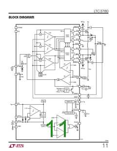
BOOST2, BOOST1 (Pins 13, 24/Pins 14, 27): Boosted
OSENSE
This pin connects the error amplifier input to an external
Floating Driver Supply. The (+) terminal of the bootstrap
resistor divider from V
.
capacitorC andC (Figure11)connectshere.TheBOOST2
OUT
A B
pin swings from a diode voltage below INTV up to V
CC
IN
SGND (Pin 7/Pin 5): Signal Ground. All small-signal com-
ponents and compensation components should connect
to this ground, which should be connected to PGND at a
single point.
+ INTV . The BOOST1 pin swings from a diode voltage
CC
below INTV up to V
+ INTV .
CC
OUT
CC
TG2,TG1(Pins14,23/Pins15,26):TopGateDrive.Drives
the top N-channel MOSFET with a voltage swing equal to
RUN (Pin 8/Pin 6): Run Control Input. Forcing the RUN
pin below 1.5V causes the IC to shut down the switching
regulatorcircuitry.Thereisa100kresistorbetweentheRUN
pin and SGND in the IC. Do not apply >6V to this pin.
INTV superimposed on the switch node voltage SW.
CC
SW2,SW1(Pins15,22/Pins17,24):SwitchNode.The(–)
terminal of the bootstrap capacitor C and C (Figure 11)
A
B
connectshere. TheSW2pinswingsfromaSchottkydiode
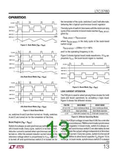
FCB (Pin 9/Pin 7): Forced Continuous Control Input. The
voltage applied to this pin sets the operating mode of the
controller. When the applied voltage is less than 0.8V, the
forced continuous current mode is active. When this pin
is allowed to float, the Burst Mode operation is active in
boost operation and the skip-cycle mode is active in buck
(external) voltage drop below ground up to V . The SW1
IN
pin swings from a Schottky diode (external) voltage drop
below ground up to V
.
OUT
BG2, BG1 (Pins 16, 18/Pins 18, 20): Bottom Gate Drive.
Drives the gate of the bottom N-channel MOSFET between
operation. When the pin is tied to INTV , the constant
ground and INTV .
CC
CC
frequency discontinuous current mode is active in buck
PGND (Pin 17/Pin 19): Power Ground. Connect this pin
or boost operation.
closelytothesourceofthebottomN-channelMOSFET,the
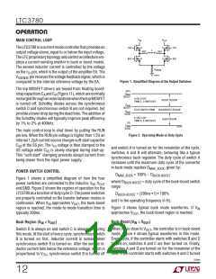
PLLFLTR (Pin 10/Pin 8): The phase-locked loop’s
lowpass filter is tied to this pin. Alternatively, this pin can
be driven with an AC or DC voltage source to vary the
frequency of the internal oscillator.
(–)terminalofC andthe(–)terminalofC (Figure11).
VCC IN
INTV (Pin19/Pin21):Internal6VRegulatorOutput. The
CC
driver and control circuits are powered from this voltage.
Bypass this pin to ground with a minimum of 4.7μF low
ESR tantalum or ceramic capacitor.
PLLIN (Pin 11/Pin 10): External Synchronization Input to
Phase Detector. This pin is internally terminated to SGND
with 50kΩ. The phase-locked loop will force the rising
bottom gate signal of the controller to be synchronized
with the rising edge of the PLLIN signal.
EXTV (Pin20/Pin22):ExternalV Input.WhenEXTV
CC
CC
CC
CC
exceeds5.7V,aninternalswitchconnectsthispintoINTV
andshutsdowntheinternalregulatorsothatthecontroller
andgatedrivepowerisdrawnfromEXTV .Donotexceed
CC
STBYMD (Pin 12/Pin 11): LDO Control Pin. Determines
whethertheinternalLDOremainsactivewhenthecontrol-
ler is shut down. See Operation section for details. If the
STBYMD pin is pulled to ground, the SS pin is internally
pulled to ground, preventing start-up and thereby provid-
ing a single control pin for turning off the controller. To
keep the LDO active when RUN is low, for example to
power a “wake up” circuit which controls the state of the
RUN pin, bypass STBYMD to signal ground with a 0.1μF
7V at this pin and ensure that EXTV < V .
CC IN
V (Pin 21/Pin 23): Main Input Supply. Bypass this pin
IN
to SGND with an RC filter (1Ω, 0.1μF).
Exposed Pad (Pin 33, QFN Only): This pin is SGND and
must be soldered to PCB ground.
capacitor, or use a resistor divider from V to keep the
pin within 2V to 5V.
IN
3780fe
10

 Linear Systems [ Linear Systems ]