LG Semicon
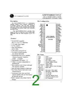
GM72V66841CT/CLT
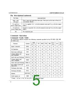
Write with auto-Precharge [WRIT A]: This
command automatically performs a Precharge
operation after a burst write with a length of 1, 2,
4 or 8, or after a single write operation. When the
burst length is full-page, this command is illegal.
Ignore command [DESL]: When this command
is set (CS is High), the synchronous DRAM
ignores command input at the Clock. However,
the internal status is held.
No operation [NOP]: This command is not an
execution command. However, the internal
operations continue.
Row address strobe and bank activate
[ACTV]: This command activates the bank that
is selected by A12/A13(BS) and determines the
row address (AX0 to AX11). If A12 is Low and
if A13 is Low, bank 0 is activated. If A12 is High
and A13 is Low, bank 1 is activated. If A12 is
Low and A13 is High, bank 2 is activated. If A12
is High and A13 is High, bank 3 is activated.
Burst stop in full page [BST]
command stops a full-page burst operation (burst
length full-page(512;GM72V66841CT/CLT)
:
This
=
and is illegal otherwise. Full page burst continues
until this command is input. When data
input/output is completed for full-page of data, it
automatically returns to the start address, and
input/output is performed repeatedly.
Precharge selected bank [PRE]: This
command starts Precharge operation for the bank
selected by A12/A13. If A12 is Low and if A13 is
Low, bank 0 is selected. If A12 is High and A13
is Low, bank 1 is selected. If A12 is Low and
A13 is High, bank 2 is selected. If A12 is High
and A13 is High, bank 3 is selected.
Column address strobe and read command
[READ]: This command starts a read operation.
In addition, the start address of burst read is
determined by the column address
AY0
to AY8; GM72V66841CT/CLT) and the
Precharge all banks [PALL]: This command
bank select address (A12/A13). After the read
operation, the output buffer becomes High-Z.
starts a Precharge operation for all banks.
Refresh [REF/SELF]: This command starts the
refresh operation. There are two types of refresh
operation, the one is auto-refresh, and the other is
self-refresh. For details, refer to the CKE truth
table section.
Read with auto-Precharge [READ A]: This
command automatically performs
a Precharge
operation after a burst read with a burst length of
1, 2, 4 or 8. When the burst length is full-page,
this command is illegal.
Mode register set [MRS]: Synchronous DRAM
has a mode register that defines how it operates.
The mode register is specified by the address pins
(A0 to A11) at the mode register set cycle. For
details, refer to the mode register configuration.
After Power on, the contents of the mode register
are undefined, execute the mode register set
command to set up the mode register.
Column address strobe and write command
[WRIT]: This command starts a write operation.
When the burst write mode is selected, the column
address (AY0 to AY8; GM72V66841CT/CLT)
and the bank select address (A12/A13) become the
burst write start address. When the single write
mode is selected, data is only written to the
location specified by the column address (AY0 to
AY8;GM72V66841CT/CLT) and the bank select
address (A12/A13).
5

 LG [ LG SEMICON CO.,LTD. ]