LG Semicon
GM72V66841CT/CLT
Pin Description(Continued)
Pin Name
DESCRIPTION
Data is input and output from these pins. These pins are the same as those of a
conventional DRAM.
DQ0 ~ DQ7
(I/O pins)
VCC and VCCQ
(Power supply pins)
3.3 V is applied. (VCC is for the internal circuit and VCCQ is for the output
buffer.)
VSS and VSSQ
Ground is connected. (VSS is for the internal circuit and VSSQ is for the output
(Power supply pins) buffer.)
NC
No Connection pins.
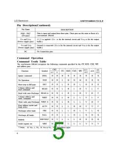
Command Operation
Command Truth Table
The synchronous DRAM recognizes the following commands specified by the CS, RAS, CAS, WE
and address pins.
CKE
A12~
A13
A0~
A11
Function
Symbol
CS RAS CAS WE
A10
n
n-1
Ignore command
No Operation
DESL
NOP
H
H
H
H
H
H
H
H
H
H
H
H
X
H
L
L
L
L
L
L
L
L
L
L
L
X
H
H
H
H
H
H
L
X
H
H
L
L
L
L
H
H
H
L
L
X
H
L
H
H
L
L
H
L
L
H
L
X
X
X
V
V
V
V
V
V
X
X
V
X
X
X
L
X
X
X
V
V
V
V
V
X
X
X
V
X
X
X
X
X
X
X
X
X
V
X
BST
Burst stop in full page
Column address and
read command
READ
READ A
WRIT
H
L
Read with auto-Precharge
Column address and
write command
WRIT A
ACTV
PRE
H
V
L
Write with auto-Precharge
Row address strobe and
bank active
L
Precharge select bank
Precharge all banks
PALL
L
H
X
V
REF/SELF
MRS
L
Refresh
L
Mode register set
* Notes : H: VIH, L: VIL, X: VIH or VIL, V: Valid address input
4

 LG [ LG SEMICON CO.,LTD. ]