LG Semicon
GM72V66841CT/CLT
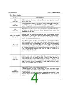
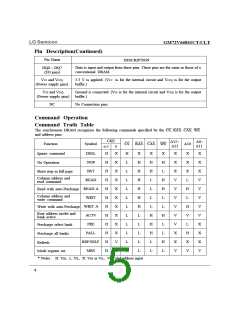
Pin Description
Pin Name
DESCRIPTION
CLK
(input pin)
CLK is the master Clock input to this pin. The other input signals are referred
at CLK rising edge.
This pin determines whether or not the next CLK is valid. If CKE is High, the
next CLK rising edge is valid. If CKE is Low, the next CLK rising edge is
invalid. This pin is used for Power-down and Clock suspend modes.
CKE
(input pin)
When CS is Low, the command input cycle becomes valid. When CS is high,
all inputs are ignored. However, internal operations (bank active, burst
operations, etc.) are held.
CS
(input pin)
Although these pin names are the same as those of conventional DRAMs,
they function in a different way. These pins define operation commands (read,
write, etc.) depending on the combination of their voltage levels. For details,
refer to the command operation section.
RAS, CAS, and WE
(input pins)
Row address (AX0 to AX11) is determined by A0 to A11 level at the bank
active command cycle CLK rising edge. Column address(AY0 to AY8;
GM72V66841CT/CLT) is determined by A0 to A8 level at the read or write
command cycle CLK rising edge. And this column address becomes burst
access start address. A10 defines the Precharge mode. When A10 = High at
the Precharge command cycle, all banks are Precharged. But when A10 =
Low at the Precharge command cycle, only the bank that is selected by
A12/A13 (BS) is Precharged.
A0 ~ A11
(input pins)
A12/A13 are bank select signal (BS). The memory array of the
GM72V66841CT/CLT is divided into bank 0, bank 1, bank2 and bank 3.
GM72V66841CT/CLT contain 4096-row x 512-column x 8-bits. If A12 is
Low and if A13 is Low, bank 0 is selected. If A12 is High and A13 is Low,
bank 1 is selected. If A12 is Low and A13 is High, bank 2 is selected. If A12
is High and A13 is High, bank 3 is selected.
A12/A13
(input pin)
DQM, DQMU/DQML controls input/output buffers.
* Read operation: If DQM, DQMU/DQML is High, The output buffer
becomes High-Z. If the DQM, DQMU/DQML is Low, the output buffer
becomes Low-Z.
* Write operation: If DQM, DQMU/DQML is High, the previous data is held
(the new data is not written). If DQM, DQMU/DQML is Low, the data is
written.
DQM,
DQMU/DQML
(input pins)
3

 LG [ LG SEMICON CO.,LTD. ]