GM72V66841CT/CLT
2,097,152 WORD x 8 BIT x 4 BANK
SYNCHRONOUS DYNAMIC RAM
LG Semicon Co.,Ltd.
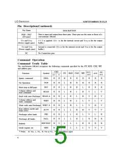
Description
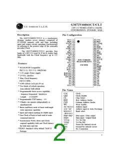
Pin Configuration
The GM72V66841CT/CLT is a synchronous
dynamic random access memory comprised of
67,108,864 memory cells and logic including
input and output circuits operating synchronously
by referring to the positive edge of the externally
provided Clock.
1
54
53
52
51
50
49
48
47
46
45
44
43
42
41
40
39
38
37
36
35
34
33
32
31
30
29
28
VCC
DQ0
VCCQ
NC
DQ1
VSSQ
NC
DQ2
VCCQ
NC
DQ3
VSSQ
NC
VCC
NC
/WE
/CAS
/RAS
/CS
VSS
DQ7
VSSQ
NC
DQ6
VCCQ
NC
DQ5
VSSQ
NC
DQ4
VCCQ
NC
VSS
NC
DQM
CLK
CKE
NC
2
3
4
5
6
7
The GM72V66841CT/CLT provides four
banks of 2,097,152 word by 8 bit to realize high
bandwidth with the Clock frequency up to 125
Mhz.
8
9
10
11
12
13
14
15
16
17
18
19
20
21
22
23
24
25
26
27
JEDEC STANDARD
400 mil 54 PIN TSOP II
Features
(TOP VIEW)
* PC100,PC66 Compatible
7K(2-2-2), 7J(3-2-2), 10K(PC66)
* 3.3V single Power supply
* LVTTL interface
BA0/A13
BA1/A12
A10,AP
A0
A11
A9
A8
A7
A6
A5
A4
* Max Clock frequency
A1
A2
A3
100/125 MHz
* 4,096 refresh cycle per 64 ms
* Two kinds of refresh operation
Auto refresh/ Self refresh
VCC
VSS
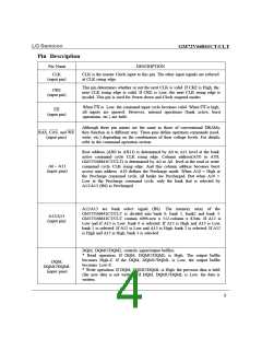
Pin Name
* Programmable burst access capability ;
- Sequence:Sequential / Interleave
- Length :1/2/4/8/FP
CLK
CKE
CS
RAS
CAS
WE
Clock
Clock Enable
Chip Select
* Programmable CAS latency : 2/3
* 4 Banks can operate independently or
simultaneously
Row Address Strobe
Column Address Strobe
Write Enable
A0~A9,A11 Address input
* Burst read/burst write or burst read/single
write operation capability
A10 / AP
BA0/A13
~BA1/A12
DQ0~DQ7
DQM
Address input or Auto Precharge
Bank select
* Input and output masking by DQM input
* One Clock of back to back read or write
command interval
Data input / Data output
Data input / output Mask
VCC for DQ
VCCQ
VSSQ
* Synchronous Power down and Clock
suspend capability with one Clock latency
for both entry and exit
VSS for DQ
VCC
VSS
NC
Power for internal circuit
Ground for internal circuit
No Connection
*JEDEC Standard 54Pin 400mil TSOP II
Package
1

 LG [ LG SEMICON CO.,LTD. ]