AN10E40 Data Manual
17
Reset Sequences
There are several sub-circuits which control the AN10E40 reset sequence and subsequent re-configuration. Each
interacts with the next to ensure reliable power up and system reset behavior.
Analog Power On Reset (APOR) & Power On Reset (POR)
When coming up cold (or at the onset of a brown out condition) the APOR circuit generates a pulse. This pulse
starts a companion 17 bit counter. This counter (driven by the internal configuration clock) serves as a digital APOR
pulse stretcher to produce a much longer POR signal to the configuration engine.
The AN10E40 provides a POR input pin so that the internal POR signal may be manually asserted. In a typical
application POR is tied to system VSS. There is otherwise rarely need for such fine control.
Internal Reset Activity
When either an external reset or internal POR reset is detected, a sequence of events transpires. First of course,
the configuration engine is reset and all the analog circuitry is powered down. Next, the configuration engine
continuously cycles through the SRAM configuration memory, repeatedly zeroing out the contents. This continues
until the 17 bit POR timer rolls over.
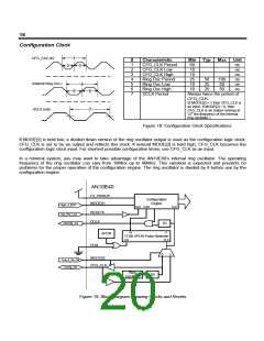
The length of the APOR pulse is dependant on VDD ramp rate, and then the entire reset process may be paced by
the widely varying ring oscillator. As such it is not possible to know a priori the exact length of the reset sequence,
but it can be bounded as shown in the performance characteristics section.
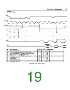
Setting MODE[2] high, and driving CFG_CLK with a known external frequency, yields a much more deterministic
configuration time. The only uncertainty is the width of the APOR pulse, but this is typically much less than half a
clock cycle.
Once the POR timer rolls over, the state of the external RESETb pin is examined. If RESETb is asserted low then
the configuration SRAM is cleared one more time and the chip is held in the reset state; configuration is held off
until RESETb is deasserted. If RESETb is instead high as the POR timer rolls over, the configuration SRAM is
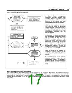
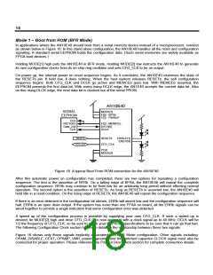
cleared on more time and the configuration sequence begins. If the chip is in BFR mode, the configuration takes
place automatically. If the chip is instead in Micro Mode, then the configuration engine waits for writes to the
function register.
External Reset Assertion
Either POR or RESETb pins can be asserted to initiate a reset. If RESETb is not asserted, then the rising edge of
POR is detected and a complete reset/configuration sequence executes. POR should be dropped before the 17 bit
counter rolls over.
If instead POR is held low, a falling edge on RESETb can be detected which will clear SRAM a single time. If
RESETb is held low, configuration is held off until RESETb is deasserted, otherwise configuration proceeds
immediately after the SRAM clear.
In BFR mode, a falling edge of the BFRb signal is detected, and it too re-initiates a configuration sequence (but no
reset sequence).
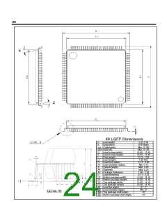
Mechanical
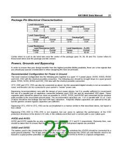
Package Details
The AN10E40 is currently offered in a 80 pin QFP package. This package has been characterized to have a ΘJA of
37 Cº/W.
There are recommendations for dry pack handling of this device. If samples or production units are received without
sealed drypack then an 8 hour, 125 ºC oven bake is recommended before wave soldering. When received in
sealed drypacks, the devices should be mounted to a PCB within 48 hours of breaking the drypack seal.

 LATTICE [ LATTICE SEMICONDUCTOR ]