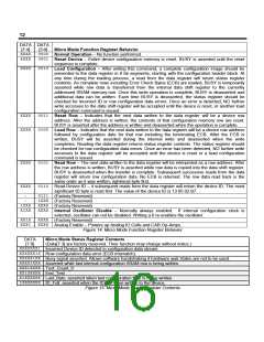
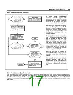
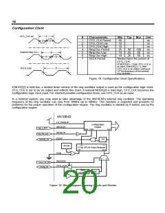
14
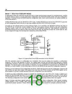
Mode 1 – Boot from ROM (BFR Mode)
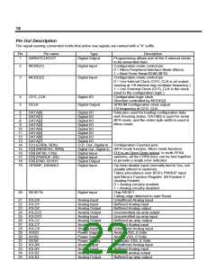
In applications where the AN10E40 should boot from a serial memory device instead of a microprocessor, connect
as shown below in Figure 16. In this stand alone configuration, the AN10E40 handles all the reset and configuration
signaling. A standard serial EEPROM holds the configuration data. (Such serial memories are widely available as
FPGA boot devices.)
Holding MODE[1] high puts the AN10E40 in BFR mode. Holding MODE[2] low instructs the AN10E40 to generate
its own configuration clocks from its on-chip ring oscillator and sets CFG_CLK to be an output.
On power up, the internal power on reset sequence begins. As it concludes, the AN10E40 examines the state of
the RESETb pin. If held low, it does nothing. When the host system releases RESETb, the self configuration
sequence begins. Both CFG_CLK and DCLK go active and MEMCEb goes low. With MEMCEb asserted, the
EEPROM presents the first data bit. With every rising DCLK edge, the AN1E40 accepts the current data bit. Also
on this rising DLCK edge, the next data bit is clocked out of the serial PROM.
AN10E40
SERIAL
MODE[1]
F[0] - BFRb
F[3] - PWRUP
EEPROM
CEb
RST/OEb
Data_Out
CLK
F[2] - MEMCEb
DATA[0]
DCLK
RESETb
CFG_CLK
RESETb
ERRb-F[1]
END-F[4]
CFG_CLK
POR
MODE[2]
Figure 16. A typical Boot From ROM connection for the AN10E40.
After this automatic power on configuration has completed, there are two options for repeating a configuration
sequence. The first is the assertion of BFRb. On a falling edge of BFRb, the AN10E40 will repeat the complete
configuration sequence. BFRb may continue to be held low for an arbitrarily long period without effecting normal
operation. The second option is the assertion of RESETb. As long as RESETb is asserted low, the AN10E40 will
hold idle in a reset condition. On the rising edge of RESETb, the AN10E40 will repeat the configuration sequence.
If there is an error detected in the configuration bit stream, ERRb will assert low and the configuration sequence will
halt. ERRb is an open drain output. If the system has more than one FPAA on board, all the ERRb signals can be
wired together to provide a single indication that some configuration error was detected.
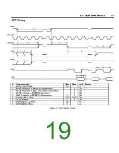
A speed up of the configuration process is possible by supplying your own CFG_CLK. If such a speed up is
desired, tie MODE[2] high and drive CFG_CLK (it is now an input) with a clock signal up to 40 MHz. DCLK will be
1/2 the frequency of CFG_CLK, so be sure to check your EEPROM specifications to be sure that it can go that fast.
The following Configuration Clock section has more detail on the relationship between these two signals.
Figure 16 shows only those signals explicitly associated with BFR Mode configuration. Other signals including:
OPAM_DISABLE, CEXT, OPAMP_VMR, powers, grounds and the switched capacitor CLOCK signal must also be
connected for proper operation. Please reference the Pin Out Description section for complete connection details.

 LATTICE [ LATTICE SEMICONDUCTOR ]