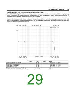
AN10E40 Data Manual
21
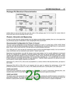
Package Pin Electrical Characterization
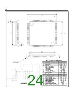
Lead Inductance
Lself [nH]
Lmutual [nH]
Center
Corner
Center
Corner
4.22
5.23
1.93
2.55
Lead Capacitance
Cself [pF]
Cmutual [pF]
Center
Corner
Center
Corner
0.52
0.61
0.18
0.26
Lead Resistance
Lead Resistance [mΩ]
Lead Impedance – Z0 [Ω]
Center
Corner
Center
Corner
1.760
2.490
90.52
92.90
Center refers to a pin to die bond wire near the center of the package (pins 10, 20, 50 and 70). Corner refers to
those bond wires near the package and die corners.
Powers, Grounds and Bypassing
In order to ensure that your design benefits from the highest possible fidelity available, there are a few signals that
you should pay special consideration to when designing the host circuit board.
Recommended Configuration for Power & Ground
The most common configuration ties the following pins together to a quiet +5 V power plane: AVDD, SVDD, BVDD
and ESD_VDD with the shortest possible connection. The following pins should be brought down to a quiet ground
plane: AVSS, SVSS, BVSS and ESD_VSS also with the shortest possible connection.
CFG_VDD and CFG_VSS can also be connected as above, but the associated digital circuitry is not as sensitive to
noise, and therefor can be connected to your system’s “noisier” power rails.
Bypassing recommendations vary with the design of your power planes, but it is usually sufficient to recommend
the use of a parallel pair of capacitors connected between each VDD pin and its associated VSS plane. These
capacitor pairs should be placed as close as possible to: AVDD, SVDD, and BVDD and connected by the shortest
path possible to the associated ground plane. The recommended capacitors are .1 uF in parallel with .01 uF. Each
of these should be low leakage and low ESR type capacitors. Polyester (Mylar) capacitors are optimal for the job,
but the generic ceramic bypass capacitors are sufficient.
Bypassing CFG_VDD to CFG_VSS can be accomplished in a manner similar to that described above, but layout is
less critical.
Bypassing ESD_VDD to ESD_VSS is not required, but can serve to optimize the performance of the ESD
protection structures in the device’s IO cells, in the unlikely event that such a current path is ever called upon.
AVDD and AVSS
AVDD and AVSS supply the op-amp and comparator circuits with +5 V and 0 V respectively. Obviously then, care
should be taken then to ensure that the quietest possible supply and ground signals are provided.
SVDD and SVSS
The wafers used in the construction of the AN10E40 are P type, so substrate ties (SVSS) should be connected to a
quiet ground potential. The N type well ties on the wafer are all connected the SVDD pin and therefor need to be
biased to a quiet positive potential. Connecting SVDD to AVDD and SVSS to AVSS is a typical configuration.

 LATTICE [ LATTICE SEMICONDUCTOR ]