AN10E40 Data Manual
13
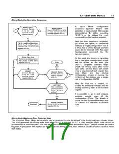
Micro Mode Configuration Sequence
A
Micro
Mode
configuration
Monitor BUSY
Detect BUSY
l i n e o r r e a d
device status
register (RS=1).
Reset Device
sequence typically begins with
assertion of device reset. This can be
accomplished by either asserting
RESETb or by writing the reset
command into the function register.
Assert RESETb or write
r e s e t c o m m a n d t o
function register (RS=0).
No
After the reset sequence completes,
you have the option to specifically
address a single configuration row at
a time, but a more typical scenario
would be to instead write the Load
Configuration command into the
function register.
Write Load Configuration
Write load configuration
c o m m a n d t o f u n c t i o n
register (RS=0).
Write Data Byte
Write next configuration
data byte to the data
register (RS=1).
At this point, the device is expecting
that a complete configuration image
will be written to the data port
(RS=1). Simplistic software might
check for device busy after every
byte write. Device busy will assert
once a long internal shift register has
been filled, and the internal
configuration engine is moving the
contents of the register into a single
row of configuration SRAM.
Stop
Error
No
BUSY?
Monitor Status
Read device
status register
(RS=1).
Detect BUSY
l i n e o r r e a d
device status
register (RS=1).
Yes
BUSY
After the final row is loaded, re-
enable the bootstrap voltage and the
analog by writing 0x10 to the function
register.
Last Data?
Has a complete
configuration
f i l e b e e n
written?
It is possible to go in and uniquely
address specific rows of the
configuration SRAM. The details of
partial on-the-fly reconfiguration may
be covered in a separate application
note.
Yes
Enable Analog
Write 0x10 to function
register (RS=0).
Finished
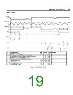
Micro Mode Maximum Data Transfer Rate
The maximum Micro Mode data transfer rate is governed by the Read and Write timing diagrams shown above.
The host processor must only write data when BUSY is inactive. BUSY is only asserted when data cannot be
accepted at the maximum rate. The host processor can either monitor the device’s BUSY output, or read the Status
Register. If processor R/W cycles are faster than the timing shown, then external circuitry must be used to insert
wait states.

 LATTICE [ LATTICE SEMICONDUCTOR ]