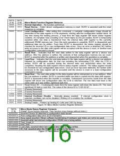
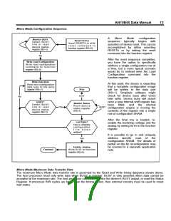
10
Mode 0 – Micro Mode
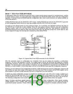
The Micro Mode interface presents a conventional asynchronous byte wide peripheral interface. When CSb is
asserted, the DATA bus is used to write commands, read status, write and read configuration data. There are two
device configuration registers, the Function register (RS=0) and the Data/Status register (RS=1). Configuration
commands are written to the Function register. Subsequent behavior is specific to the command issued and is
documented in Figure 14.
The Data/Status register is either used to read or write configuration data or read device status. By popular
convention, RS is typically connected to the least significant bit of the processor’s address bus to map the Function
register to an even address and the Data/Status register to an odd address.
Figure 12 shows only those signals explicitly associated with Micro Mode configuration. Other signals including:
POR, OPAM_DISABLE, CEXT, OPAMP_VMR, powers, grounds and the switched capacitor CLOCK signal must
also be connected for proper operation. Please reference the Pin Out Description section for complete connection
details.
AN10E40
MODE[2]
F[0] - CSb
Microprocessor
Addr[n:0]
A[0]
F[3] - RS
WRITEb
READb
WAIT
F[2] - WRb
F[1] - RDb
F[4] - BUSY
D[7:0]
DATA[7:0]
CLK
CFG_CLK
RESETb
RESETb
MODE[1]
CLK
RSTb
Figure 12. A conventional microprocessor interface for configuring AN10E40.

 LATTICE [ LATTICE SEMICONDUCTOR ]