AN10E40 Data Manual
9
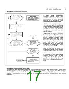
Configuration Engine
The AN10E40 provides two modes of operation for loading the configuration SRAM. The simplest is Mode 1, Boot
From Serial ROM. This is the most common method of booting conventional SRAM based FPGA’s so consequently
the cost of compatible low pin count serial PROMs has been driven way down. Some designs may however want to
take advantage of the AN10E40’s on the fly reprogrammability. In this case the Micro Mode (Mode 0) may be the
appropriate configuration interface.
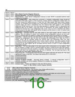
MODE
Pins
[2] [1] Description
x
x
0
1
0
1
x
x
Mode 0 – Micro Mode, a conventional byte wide microprocessor interface
Mode 1 – Boot from Serial PROM (a.k.a. Boot from ROM or BFR Mode)
AN10E40 generates its own configuration clocks (using an internal oscillator). CFG_CLK is an output.
Use an external clock for configuration. CFG_CLK is the input.
Figure 10. Mode Pin Settings for Configuration Options
The configuration SRAM for the AN10E40 contains 6864 bits. Configuration files will be slightly larger to facilitate
byte alignment of data as well as address and checksum information.
The pins involved with configuration of the device are given in the following table. The F[4:0] pins change behavior
based on the setting of the MODE[2:1] pins. The signal naming convention holds that active low signals are named
with a “b” suffix.
Pins Common to Configuration Modes
Pin Name
MODE[2:1]
CFG_CLK
Description
I
Used to establish the configuration mode.
I/O If MODE[2] is high, then configuration clock input, otherwise configuration clock output.
Pins used in Micro Mode (Mode 0)
POR
I
I
Complete chip reset sequence begins on rising edge of POR. (Usually tied low.)
Reset sequence begins on falling edge. Chip held in reset state as long as asserted low.
Configuration re-starts on release of RESETb.
RESETb
F[0] CSb
F[1] RDb
F[2] WRb
F[3] RS
I
I
When low, selects the AN10E40 for a data transfer transaction
Assert low for a Read transaction.
I
Assert low for a Write transaction.
I
Register Select. RS=0 to select Function register. RS=1 to select Data/Status register.
Asserted high when the device is not ready to accept data, i.e. while device is resetting,
or a data shift register to configuration SRAM transfer is taking place.
F[4] BUSY
O
DATA[7:0]
I/O Byte wide bi-directional data port
Pins used in BFR Mode (Mode 1)
POR
I
Complete chip reset sequence begins on rising edge of POR. Once complete, the
configuration sequence begins. (Usually tied low.)
Reset sequence begins on falling edge. Chip held in reset state as long as asserted low.
Configuration re-starts on release of RESETb.
RESETb
I
F[0] BFRb
F[1] ERRb
F[2] MEMCEb
F[3] PWRUP
F[4] END
I
On falling edge of BFRb, configuration sequence occurs.
Asserts low if a an error is detected in the configuration data stream. (Open Drain)
Asserts low to select the external memory device.
Tie to VDD.
O
O
I
O
O
I
Asserts high to signify configuration has completed.
Data clock to serial PROM.
DCLK
DATA[0]
Bit wide data input.
Figure 11. Configuration Pin Functions

 LATTICE [ LATTICE SEMICONDUCTOR ]