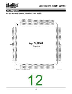
Specifications ispLSI 3256A
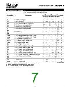
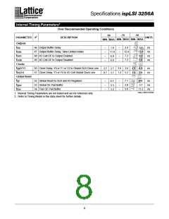
Internal Timing Parameters1
Over Recommended Operating Conditions
-70
-50
-90
2
PARAMETER
Outputs
#
DESCRIPTION
UNITS
MIN. MAX. MIN. MAX.
MIN. MAX.
46 Output Buffer Delay
–
–
–
–
2.4
12.4
7.2
–
–
–
–
3.3
13.3
9.8
ns
ns
ns
ns
t
t
t
t
ob
–
–
–
–
1.9
11.9
6.8
47 Output Buffer Delay, Slew Limited Adder
48 I/O Cell OE to Output Enabled
obs
oen
odis
49 I/O Cell OE to Output Disabled
7.2
9.8
6.8
Clocks
t
t
gy0/1/2
ioy3/4
50 Clock Delay, Y0 or Y1 or Y2 to Global GLB Clock Line
51 Clock Delay, Y3 or Y4 to I/O Cell Global Clock Line
3.6 3.6 4.9 4.9
1.2 5.2 1.6 7.0
ns
ns
2.7 2.7
0.7 3.7
Global Reset
52 Global Reset to GLB and I/O Registers
53 Global OE Pad Buffer
7.1
2.8
9.8
–
–
–
9.6
3.7
ns
ns
ns
t
t
t
gr
–
–
–
6.7
2.3
3.2
–
–
–
goe
toe
54 Test OE Pad Buffer
13.2
Table 2-0037C/3256A
1. Internal Timing Parameters are not tested and are for reference only.
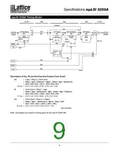
2. Refer to Timing Model in this data sheet for further details.
8

 LATTICE [ LATTICE SEMICONDUCTOR ]