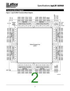
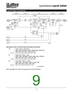
Specifications ispLSI 3256A
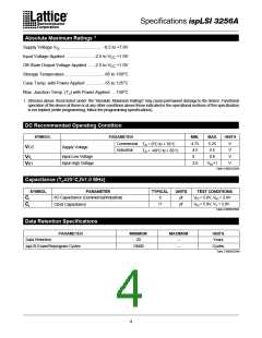
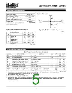
Switching Test Conditions
Figure 2. Test Load
Input Pulse Levels
GND to 3.0V
≤ 3ns 10% to 90%
1.5V
+ 5V
Input Rise and Fall Time
Input Timing Reference Levels
Output Timing Reference Levels
Output Load
R
1
2
1.5V
Device
Output
Test
Point
See Figure 2
Table 2-0003/3256A
3-state levels are measured 0.5V from
steady-state active level.
R
C *
L
Output Load conditions (See Figure 2)
*
C includes Test Fixture and Probe Capacitance.
L
0213A
TEST CONDITION
R1
470Ω
∞
R2
CL
A
B
390Ω
390Ω
390Ω
35pF
35pF
35pF
Active High
Active Low
470Ω
Active High to Z
∞
390Ω
390Ω
5pF
at VOH-0.5V
C
Active Low to Z
at VOL+0.5V
470Ω
5pF
Table 2 - 0004A
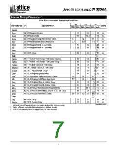
DC Electrical Characteristics
Over Recommended Operating Conditions
3
SYMBOL
PARAMETER
Output Low Voltage
Output High Voltage
CONDITION
IOL= 8 mA
MIN.
–
TYP. MAX. UNITS
–
–
0.4
–
V
VOL
IOH = -4 mA
2.4
–
V
VOH
Input or I/O Low Leakage Current
Input or I/O High Leakage Current
ispEN Input Low Leakage Current
I/O Active Pull-Up Current
0V ≤ V ≤ V (Max.)
–
-10
10
µA
µA
µA
µA
mA
mA
mA
I
I
I
I
I
IL
IH
IN
IL
3.5V ≤ V ≤ V
–
–
IN
CC
0V ≤ V ≤ V
–
–
-150
-150
-200
–
IL-isp
IL-PU
OS1
IN
IL
0V ≤ V ≤ V
–
–
IN
IL
Output Short Circuit Current
VCC= 5V, VOUT = 0.5V
–
–
–
200
200
V = 0.0V, V = 3.0V
Commercial
Industrial
CC2, 4
IL
IH
Operating Power Supply Current
I
–
–
fCLOCK = 1 MHz
Table 2-0007/3256A
1. One output at a time for a maximum duration of one second. VOUT = 0.5V was selected to avoid test problems
by tester ground degradation. Characterized but not 100% tested.
2. Measured using 16 16-bit counters.
3. Typical values are at VCC= 5V and T = 25°C.
A
4. Maximum ICC varies widely with specific device configuration and operating frequency. Refer to the Power Consumption
section of this data sheet and Thermal Management section of the Lattice Semiconductor Data Book or CD-ROM to
estimate maximum ICC
.
5

 LATTICE [ LATTICE SEMICONDUCTOR ]