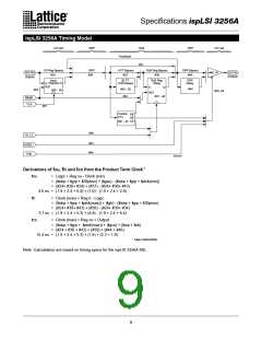
Specifications ispLSI 3256A
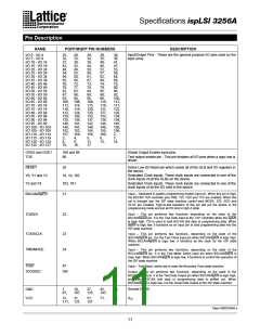
Pin Description
NAME
PQFP/MQFP PIN NUMBERS
DESCRIPTION
I/O 0 - I/O 4
I/O 5 - I/O 9
25,
32,
37,
42,
48,
54,
59,
65,
70,
76,
82,
87,
93,
106, 108,
113, 114,
118, 119,
123, 124,
129, 130,
135, 136,
140, 141,
146, 147,
152, 153,
157, 158,
26,
33,
38,
43,
49,
55,
60,
66,
72,
77,
83,
88,
94,
28,
34,
39,
44,
50,
56,
61,
67,
73,
78,
84,
89,
29,
35,
40,
46,
52,
57,
62,
68,
74,
79,
85,
90,
30,
36,
41,
47,
53,
58,
64,
69,
75,
80,
86,
92,
105,
112,
117,
122,
128,
134,
139,
145,
150,
156,
2,
Input/Output Pins - These are the general purpose I/O pins used by the
logic array.
I/O 10 - I/O 14
I/O 15 - I/O 19
I/O 20 - I/O 24
I/O 25 - I/O 29
I/O 30 - I/O 34
I/O 35 - I/O 39
I/O 40 - I/O 44
I/O 45 - I/O 49
I/O 50 - I/O 54
I/O 55 - I/O 59
I/O 60 - I/O 64
I/O 65 - I/O 69
I/O 70 - I/O 74
I/O 75 - I/O 79
I/O 80 - I/O 84
I/O 85 - I/O 89
I/O 90 - I/O 94
I/O 95 - I/O 99
I/O 100 - I/O 104
I/O 105 - I/O 109
I/O 110 - I/O 114
I/O 115 - I/O 119
I/O 120 - I/O 124
I/O 125 - I/O 127
95,
96,
109,
115,
120,
126,
132,
137,
142,
148,
154,
159,
5,
110,
116,
121,
127,
133,
138,
144,
149,
155,
160,
6,
3,
8,
15,
4,
9,
16,
7,
14,
11,
17
13,
GOE0 and GOE1
TOE
100 and 99
98
Global Output Enable input pins.
Test output enable pin - This pin tristates all I/O pins when a logic low is
driven
RESET
20
Active Low (0) Reset pin which resets all of the GLB and I/O registers in
the device.
Y0, Y1 and Y2
Y3 and Y4
18, 19, 103
102, 101
Dedicated Clock inputs. These clock inputs are connected to one of the
clock inputs of all the GLBs on the device.
Dedicated Clock inputs. These clock inputs are connected to one of the
clock inputs of all the I/O cells in the device.
Input – Dedicated in-system programming enable input pin. When this pin is high,
the BSCAN TAP controller pins TMS, TDI, TDO and TCK are enabled. When this
pin is brought low, the ISP state machine control pins MODE, SDI, SDO and
SLCK are enabled. High-to-low transition of this pin will put the device in the
programming mode and put all I/O pins in high-Z state.
BSCAN/ispEN
21
Input
– This pin performs two functions depending on the state of the
TDI/SDI
22
BSCAN/ispEN pin. It is the Test Data input to the TAP Controller when the ispEN
is logic high. TDI is used to load BSCAN test data or programming data. When
ispEN is logic low, it functions as an input pin to load programming data into the
ISP state machine.
Input
– This pin performs two functions, depending on the state of the
TCK/SCLK
23
24
BSCAN/ispEN pin. It is the Test Clock input pin when BSCAN/ispEN is logic high.
When BSCAN/ispEN is logic low, it functions as the clock for the ISP state
machine.
TMS/MODE
Input
– This pin performs two functions, depending on the state of the
BSCAN/ispEN pin. It is the Test Mode Select input pin when BSCAN/ispEN is
logic high. When BSCAN/ispEN is logic low, it functions to control the operation of
the ISP state machine.
97
TRST
Input – Test Reset, active low to reset the Boundary Scan state machine.
TDO/SDO
104
Output – This pin performs two functions, depending on the state of the
BSCAN/ispEN pin. It is the Test Data Output pin when BSCAN/ispEN is logic high,
and either BSCAN test data or programming data is shifted out. When
BSCAN/ispEN is logic low, it is the Serial Data Output of the ISP state machine.
GND
VCC
1,
81,
10,
107,
27,
125,
45,
143
63,
91,
Ground (GND)
VCC
12,
111, 131,
31,
51,
151
71,
Table 2-0002/3256A.a
11

 LATTICE [ LATTICE SEMICONDUCTOR ]