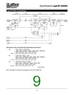
Specifications ispLSI 3256A
1
Absolute Maximum Ratings
Supply Voltage V .................................. -0.5 to +7.0V
cc
Input Voltage Applied........................ -2.5 to V +1.0V
CC
Off-State Output Voltage Applied ..... -2.5 to V +1.0V
CC
Storage Temperature................................ -65 to 150°C
Case Temp. with Power Applied .............. -55 to 125°C
Max. Junction Temp. (T ) with Power Applied ... 150°C
J
1. Stresses above those listed under the “Absolute Maximum Ratings” may cause permanent damage to the device. Functional
operation of the device at these or at any other conditions above those indicated in the operational sections of this specification
is not implied (while programming, follow the programming specifications).
DC Recommended Operating Condition
SYMBOL
PARAMETER
Commercial
Industrial
MIN.
4.75
4.5
0
MAX.
5.25
5.5
UNITS
V
V
V
V
T
T
= 0°C to + 70°C
A
VCC
Supply Voltage
= -40°C to + 85°C
A
Input Low Voltage
Input High Voltage
0.8
VIL
2.0
V +1
cc
VIH
Table 2-0005/3256A
Capacitance (TA=25°C,f=1.0 MHz)
SYMBOL
PARAMETER
TYPICAL
UNITS
TEST CONDITIONS
CC= 5.0V, VI/O = 2.0V
VCC= 5.0V, VY = 2.0V
9
pf
pf
V
I/O Capacitance (Commercial/Industrial)
Clock Capacitance
C1
C2
11
Table 2-0006/3256A
Data Retention Specifications
PARAMETER
Data Retention
MINIMUM
20
MAXIMUM
UNITS
Years
Cycles
–
–
ispLSI Erase/Reprogram Cycles
10000
Table 2-0008/3256A
4

 LATTICE [ LATTICE SEMICONDUCTOR ]