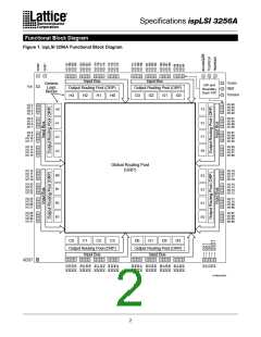
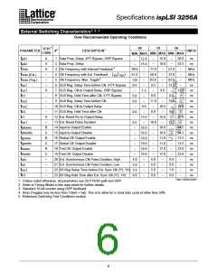
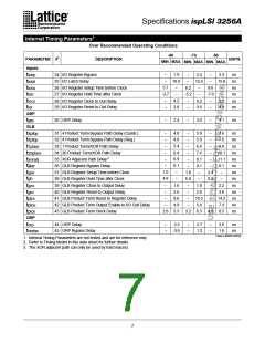
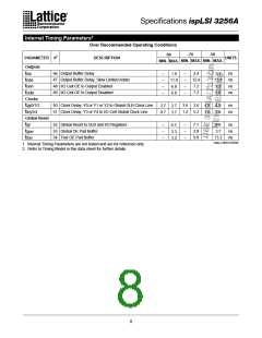
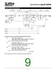
Specifications ispLSI 3256A
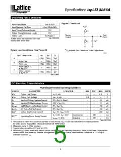
External Switching Characteristics1, 2, 3
Over Recommended Operating Conditions
TEST5
COND.
-70
-50
-90
DESCRIPTION1
UNITS
2
PARAMETER
#
MIN. MAX. MIN. MAX.
MIN. MAX.
A
A
A
–
1 Data Prop. Delay, 4PT Bypass, ORP Bypass
2 Data Prop. Delay
3 Clk Frequency with Internal Feedback3
–
–
15.0
18.0
–
–
–
20.0
24.5
–
ns
ns
–
–
12.0
15.0
–
t
t
f
f
f
t
t
t
t
t
t
t
t
t
t
t
t
t
t
t
t
t
t
pd1
pd2
77.0
50.0
83.0
9.5
–
57.0
37.0
63.0
12.5
–
MHz
MHz
MHz
ns
90.0
61.0
125
8.0
–
max
1
4 Clk Frequency with Ext. Feedback
5 Clk Frequency, Max. Toggle4
(
)
–
–
–
max (Ext.)
max (Tog.)
su1
tsu2 + tco1
–
–
–
–
–
6 GLB Reg. Setup Time before Clk, 4 PT Bypass
7 GLB Reg. Clk to Output Delay, ORP Bypass
8 GLB Reg. Hold Time after Clk, 4 PT Bypass
9 GLB Reg. Setup Time before Clk
10 GLB Reg. Clk to Output Delay
–
–
–
A
–
9.0
–
12.0
–
ns
7.5
–
co1
0.0
11.0
–
0.0
15.0
–
ns
h1
0.0
9.0
–
–
–
–
ns
–
su2
–
10.5
–
14.0
–
ns
co2
9.0
–
–
11 GLB Reg. Hold Time after Clk
0.0
–
0.0
–
ns
h2
0.0
–
A
–
12 Ext. Reset Pin to Output Delay
13 Ext. Reset Pulse Duration
15.0
–
20.0
–
ns
13.5
–
r1
10.0
–
13.5
–
ns
6.5
–
rw1
B
C
B
C
B
C
–
14 Input to Output Enable
18.0
18.0
11.0
11.0
17.0
17.0
–
24.5
24.5
13.5
13.5
23.0
23.0
–
ns
16.0
16.0
10.0
10.0
10.0
10.0
–
ptoeen
ptoedis
goeen
goedis
toeen
toedis
wh
15 Input to Output Disable
–
–
ns
–
16 Global OE Output Enable
–
–
ns
–
17 Global OE Output Disable
–
–
ns
–
18 Test OE Output Enable
–
–
ns
–
19 Test OE Output Disable
–
–
ns
–
20 Ext. Synchronous Clk Pulse Duration, High
21 Ext. Synchronous Clk Pulse Duration, Low
22 I/O Reg Setup Time before Ext. Sync Clk (Y3, Y4)
23 I/O Reg Hold Time after Ext. Sync Clk (Y3, Y4)
6.0
6.0
5.0
0.0
8.0
8.0
7.0
0.0
ns
4.0
4.0
5.0
0.0
–
–
–
ns
–
wl
–
–
–
ns
–
su3
–
–
–
ns
–
h3
Table 2-0030C/3256A
1. Unless noted otherwise, all parameters use 20 PTXOR path and ORP.
2. Refer to Timing Model in this data sheet for further details.
3. Standard 16-bit counter using GRP feedback.
4. fmax (Toggle) may be less than 1/(twh + twl). This is to allow for a clock duty cycle of other than 50%.
5. Reference Switching Test Conditions section.
6

 LATTICE [ LATTICE SEMICONDUCTOR ]