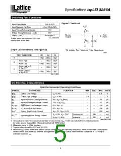
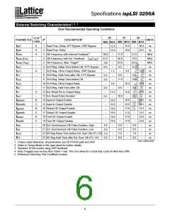
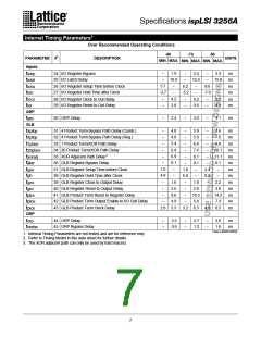
Specifications ispLSI 3256A
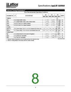
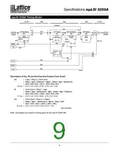
ispLSI 3256A Timing Model
I/O Cell
GRP
GLB
#31
ORP
I/O Cell
Feedback
I/O Reg Bypass
#24
GRP
#30
4 PT Bypass
#32
GLB Reg Bypass
#36
ORP Bypass
#45
#46, 47
I/O Pin
I/O Pin
(Input)
(Output)
Input
Register
20 PT
XOR Delays
GLB Reg
Delay
ORP
Delay
Q
D
RST
D
Q
#44
#33 - 35
#52
#52
#25 - 29
#48, 49
RST
#37 - 40
Reset
Y3,4
#51
Control
PTs
RE
OE
CK
#41 - 43
#50
Y0,1,2
#53
#54
GOE0,1
TOE
0902/3256A
Derivations of tsu, th and t
co from the Product Term Clock1
t
t
t
su
= Logic + Reg su - Clock (min)
= ( iobp + grp + 20ptxor) + ( gsu) - (tiobp + tgrp + tptck(min))
= (#24+ #30+ #34) + (#37) - (#24+ #30+ #43)
t
t
t
t
4.6 ns = (1.9 + 2.4 + 6.4) + (1.0) - (1.9 + 2.4 + 2.8)
h
= Clock (max) + Reg h - Logic
= (tiobp + tgrp + tptck(max)) + (tgh) - (tiobp + tgrp + t20ptxor)
= (#24+ #30+ #43) + (#38) - (#24+ #30+ #34)
3.7 ns = (1.9 + 2.4 + 5.3) + (4.8) - (1.9 + 2.4 + 6.4)
co
= Clock (max) + Reg co + Output
= (
= (#24 + #30 + #43) + (#39) + (#44 + #46)
15.4 ns = (1.9 + 2.4 + 5.3) + (1.6) + (2.3 + 1.9)
tiobp + tgrp + tptck(max)) + (tgco) + (torp + tob)
Table 2-0042/3256A
Note: Calculations are based on timing specs for the ispLSI 3256A-90L.
9

 LATTICE [ LATTICE SEMICONDUCTOR ]