LANSDALE Semiconductor, Inc.
ML1451xx
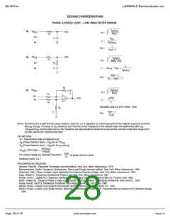
CRYSTAL OSCILLATOR CONSIDERATIONS
The following options may be considered to provide a refer-
ence frequency to Motorola's or Lansdale’s CMOS frequency
synthesizers.
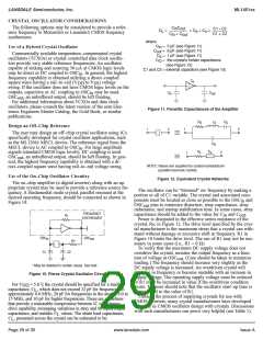
C C
in out
C1 • C2
C1 + C2
C =
L
+ C + C +
a o
C
+ C
out
in
where
C
= 5 pF (see Figure 11)
= 6 pF (see Figure 11)
Use of a Hybrid Crystal Oscillator
in
C
out
Commercially available temperature–compensated crystal
oscillators (TCXOs) or crystal–controlled data clock oscilla-
tors provide very stable reference frequencies. An oscillator
capable of sinking and sourcing 50 µA at CMOS logic levels
C = 1 pF (see Figure 11)
a
C
= the crystal's holder capacitance
(see Figure 12)
O
C1 and C2 = external capacitors (see Figure 10)
may be direct or DC coupled to OSC . In general, the highest
in
frequency capability is obtained utilizing a direct–coupled
C
a
square wave having a rail–to–rail (V
to V ) voltage
DD
SS
swing. If the oscillator does not have CMOS logic levels on the
outputs, capacitive or AC coupling to OSC may be used.
C
C
out
in
in
OSC , an unbuffered output, should be left floating.
out
For additional information about TCXOs and data clock
oscillators, please consult the latest version of the eem Elec-
tronic Engineers Master Catalog, the Gold Book, or similar
publications.
Figure 11. Parasitic Capacitances of the Amplifier
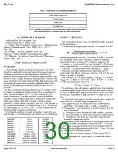
R
L
C
S
S
S
Design an Off–Chip Reference
1
2
1
2
The user may design an off–chip crystal oscillator using ICs
specifically developed for crystal oscillator applications, such
as the ML12061 MECL device. The reference signal from the
C
O
MECL device is AC coupled to OSC . For large amplitude
in
R
X
e
signals (standard CMOS logic levels), DC coupling is used.
e
2
1
OSC , an unbuffered output, should be left floating. In gen-
out
eral, the highest frequency capability is obtained with a di-
rect–coupled square wave having rail–to–rail voltage swing.
NOTE: Values are supplied by crystal manufacturer
(parallel resonant crystal).
Use of the On–Chip Oscillator Circuitry
Figure 12. Equivalent Crystal Networks
The on–chip amplifier (a digital inverter) along with an ap-
propriate crystal may be used to provide a reference source fre-
quency. A fundamental mode crystal, parallel resonant at the
desired operating frequency, should be connected as shown in
Figure 10.
The oscillator can be “trimmed” on–frequency by making a
portion or all of C1 variable. The crystal and associated com-
ponents must be located as close as possible to the OSC and
in
OSC
out
pins to minimize distortion, stray capacitance, stray
inductance, and startup stabilization time. In some cases, stray
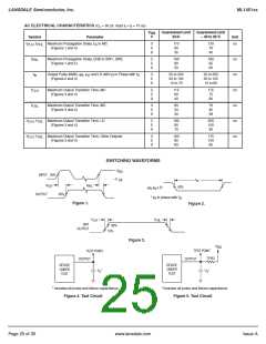
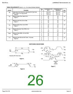
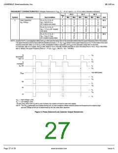
FREQUENCY
SYNTHESIZER
capacitance should be added to the value for C and C
.
R
in out
f
Power is dissipated in the effective series resistance of the
crystal, Re, in Figure 12. The drive level specified by the crys-
tal manufacturer is the maximum stress that a crystal can with-
stand without damage or excessive shift in frequency. R1 in
Figure 10 limits the drive level. The use of R1 may not be nec-
essary in some cases (i.e., R1 = 0 Ω).
OSC
C1
OSC
out
in
R1*
To verify that the maximum DC supply voltage does not
overdrive the crystal, monitor the output frequency as a func-
C2
tion of voltage at OSC . (Care should be taken to minimize
out
loading.) The frequency should increase very slightly as the
DC supply voltage is increased. An overdriven crystal will
decrease in frequency or become unstable with an increase in
supply voltage. The operating supply voltage must be reduced
or R1 must be increased in value if the overdriven condition
exists. The user should note that the oscillator start–up time is
proportional to the value of R1.
Through the process of supplying crystals for use with
CMOS inverters, many crystal manufacturers have developed
expertise in CMOS oscillator design with crystals. Discussions
with such manufacturers can prove very helpful (see Table 1).
* May be deleted in certain cases. See text.
Figure 10. Pierce Crystal Oscillator Circuit
For V
DD
= 5.0 V, the crystal should be specified for a loading
capacitance, C , which does not exceed 32 pF for frequencies to
L
approximately 8.0 MHz, 20 pF for frequencies in the area of 8.0 to
15 MHz, and 10 pF for higher frequencies. These are guidelines
that provide a reasonable compromise between IC capacitance,
drive capability, swamping variations in stray and IC input/output
capacitance, and realistic C values. The shunt load capacitance,
L
C , presented across the crystal can be estimated to be:
L
Page 29 of 35
www.lansdale.com
Issue A

 LANSDALE [ LANSDALE SEMICONDUCTOR INC. ]