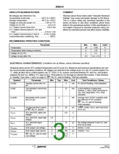
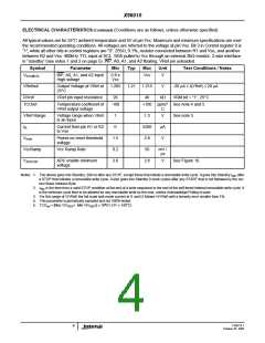
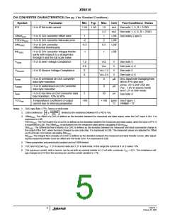
X96010
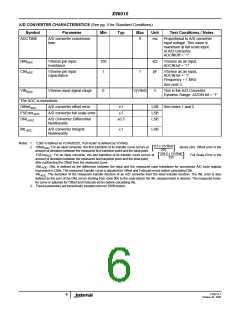
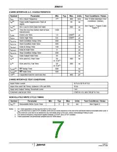
2-WIRE INTERFACE A.C. CHARACTERISTICS
Symbol
Parameter
SCL Clock Frequency
Min
1(3)
Typ Max
Units Test Conditions / Notes
fSCL
400
50
kHz
ns
See “2-Wire Interface Test
Conditions” (below),
(4)
tIN
Pulse width Suppression Time at
inputs
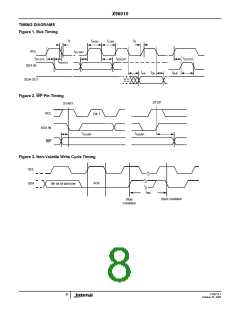
See Figure 1, Figure 2 and
Figure 3.
(4)
tAA
SCL Low to SDA Data Out Valid
900
ns
ns
(4)
tBUF
Time the bus free before start of new
transmission
1300
tLOW
Clock Low Time
1.3
0.6
600
600
100
0
1200(3)
1200(3)
µs
µs
ns
ns
ns
µs
ns
ns
ns
tHIGH
Clock High Time
tSU:STA
tHD:STA
tSU:DAT
tHD:DAT
tSU:STO
tDH
Start Condition Setup Time
Start Condition Hold Time
Data In Setup Time
Data In Hold Time
Stop Condition Setup Time
Data Output Hold Time
SDA and SCL Rise Time
600
50
(4)
tR
20
300
300
+0.1Cb(1)
(4)
tF
SDA and SCL Fall Time
20
ns
+0.1Cb(1)
(4)
tSU:WP
WP Setup Time
600
600
ns
ns
pF
(4)
tHD:WP
WP Hold Time
Cb(4)
Capacitive load for each bus line
400
2-WIRE INTERFACE TEST CONDITIONS
Input Pulse Levels
10 % to 90 % of Vcc
Input Rise and Fall Times, between 10% and 90%
Input and Output Timing Threshold Level
External Load at pin SDA
10 ns
1.4V
2.3kΩ to Vcc and 100 pF to Vss
NONVOLATILE WRITE CYCLE TIMING
Symbol
Parameter
Min
Typ
Max
Units
Test Conditions / Notes
See Figure 3
(2)
tWC
Nonvolatile Write Cycle Time
5
10
ms
Notes: 1. Cb = total capacitance of one bus line (SDA or SCL) in pF.
2. WC is the time from a valid STOP condition at the end of a write sequence to the end of the self-timed internal nonvolatile write cycle. It
is the minimum cycle time to be allowed for any nonvolatile write by the user, unless Acknowledge Polling is used.
t
3. The minimum frequency requirement applies between a START and a STOP condition.
4. These parameters are periodically sampled and not 100% tested.
FN8214.1
7
October 25, 2005

 INTERSIL [ Intersil ]