X96010
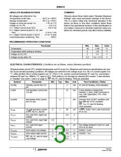
ABSOLUTE MAXIMUM RATINGS
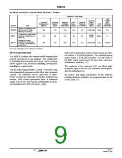
COMMENT
All voltages are referred to Vss.
Stresses above those listed under “Absolute Maximum
Ratings” may cause permanent damage to the device.
This is a stress rating only; functional operation of the
device (at these or any other conditions above those
listed in the operational sections of this specification) is
not implied. Exposure to absolute maximum rating con-
ditions for extended periods may affect device reliability.
Temperature under bias ................... -65°C to +100°C
Storage temperature ........................ -65°C to +150°C
Voltage on every pin except Vcc................ -1.0V to +7V
Voltage on Vcc Pin .............................................0 to 5.5V
D.C. Output Current at pin SDA...................... 0 to 5 mA
D.C. Output Current at pins R1, R2, and
VRef........................................................ -0.50 to 1 mA
D.C. Output Current at pins I1 and I2 ....... -3.5 to +3.5mA
Lead temperature (soldering, 10s) .................... 300°C
RECOMMENDED OPERATING CONDITIONS
Parameter
Temperature
Min.
-40
0
Max.
+100
Units
°C
Temperature while writing to memory
Voltage on Vcc Pin
+70
°C
3
5.5
V
Voltage on any other Pin
-0.3
Vcc + 0.3
V
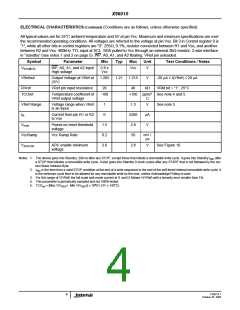
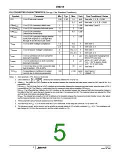
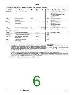
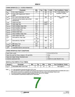
ELECTRICAL CHARACTERISTICS (Conditions are as follows, unless otherwise specified)
All typical values are for 25°C ambient temperature and 5V at pin Vcc. Maximum and minimum specifications are over
the recommended operating conditions. All voltages are referred to the voltage at pin Vss. Bit 3 in Control register 0 is
“1”, while all other bits in control registers are “0”. 255Ω, 0.1%, resistor connected between R1 and Vss, and another
between R2 and Vss. 400kHz TTL input at SCL. SDA pulled to Vcc through an external 2kΩ resistor. 2-wire interface
in “standby” (see notes 1 and 2 on page 5). WP, A0, A1, and A2 floating. VRef pin unloaded.
Symbol
Iccstby
Parameter
Min
Typ
Max
Unit
Test Conditions / Notes
Standby current into Vcc
pin
2
mA
R1 and R2 floating, VRef unloaded.
Iccfull
Full operation current into
Vcc pin
15
mA
mA
2-wire interface reading from
memory, I1 and I2 both connected to
Vss, DAC input bytes: FFh, VRef
unloaded.
Iccwrite
Nonvolatile Write current
into Vcc pin
4
1
Average from START condition until
tWP after the STOP condition
WP: Vcc, R1 and R2 floating,
VRef unloaded.
IPLDN
VILTTL
VIHTTL
IINTTL
On-chip pull down current
at WP, A0, A1, and A2
0
20
µA
V
V(WP), V(A0), V(A1), and V(A2) from
0V to Vcc
SCL and SDA, input Low
voltage
0.8
SCL and SDA, input High
voltage
2.0
-1
V
SCL and SDA input
current
10
µA
Pin voltage between 0 and Vcc, and
SDA as an input.
VOLSDA
IOHSDA
VILCMOS
SDA output Low voltage
SDA output High current
0
0
0
0.4
V
µA
V
I(SDA) = 2 mA
V(SDA) = Vcc
100
WP, A0, A1, and A2 input
Low voltage
0.2 x
Vcc
FN8214.1
October 25, 2005
3

 INTERSIL [ Intersil ]