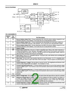
X96010
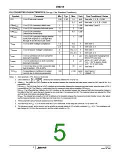
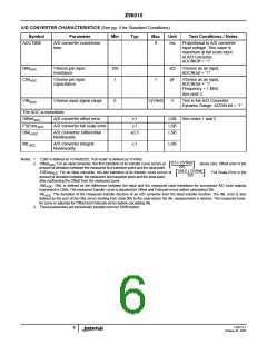
A/D CONVERTER CHARACTERISTICS (See pg. 4 for Standard Conditions)
Symbol
Parameter
Min
Typ
Max
Unit
Test Conditions / Notes
ADCTIME
A/D converter conversion
time
9
ms
Proportional to A/D converter
input voltage. This value is
maximum at full scale input
of A/D converter.
ADCfiltOff = “1”
RINADC
CINADC
VSense pin input
resistance
100
1
kΩ
VSense as an input,
ADCIN bit = “1”
VSense pin input
capacitance
7
pF
VSense as an input,
ADCIN bit = “1”,
Frequency = 1 MHz
See note 3.
VINADC
VSense input signal range
0
V(VRef)
V
This is the A/D Converter
Dynamic Range. ADCIN bit = “1”
The ADC is monotonic
OffsetADC
FSErrorADC
DNLADC
A/D converter offset error
±1
±1
LSB See notes 1 and 2
A/D converter full scale error
LSB
LSB
A/D Converter Differential
Nonlinearity
±0.5
INLADC
A/D converter Integral
Nonlinearity
±1
LSB
Notes: 1. “LSB” is defined as V(VRef)/255, “Full Scale” is defined as V(VRef).
0.5 x V(VRef)
2. OffsetADC: For an ideal converter, the first transition of its transfer curve occurs at
amount of deviation between the measured first transition point and the ideal point.
above zero. Offset error is the
[
]
255
254.5 x V(VRef)
255
FSErrorADC: For an ideal converter, the last transition of its transfer curve occurs at
amount of deviation between the measured last transition point and the ideal point,
after subtracting the Offset from the measured curve.
. Full Scale Error is the
[
]
DNLADC: DNL is defined as the difference between the ideal and the measured code transitions for successive A/D code outputs
expressed in LSBs. The measured transfer curve is adjusted for Offset and Fullscale errors before calculating DNL.
INLADC: The deviation of the measured transfer function of an A/D converter from the ideal transfer function. The INL error is also
defined as the sum of the DNL errors starting from code 00h to the code where the INL measurement is desired. The measured trans-
fer curve is adjusted for Offset and Fullscale errors before calculating INL.
3. These parameters are periodically sampled and not 100% tested.
FN8214.1
6
October 25, 2005

 INTERSIL [ Intersil ]