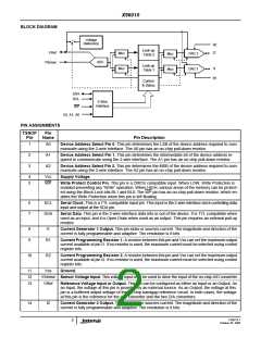
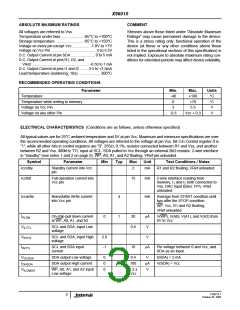
X96010
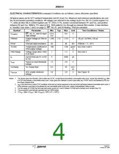
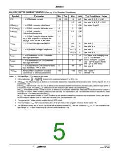
ELECTRICAL CHARACTERISTICS (Continued) (Conditions are as follows, unless otherwise specified)
All typical values are for 25°C ambient temperature and 5V at pin Vcc. Maximum and minimum specifications are over
the recommended operating conditions. All voltages are referred to the voltage at pin Vss. Bit 3 in Control register 0 is
“1”, while all other bits in control registers are “0”. 255Ω, 0.1%, resistor connected between R1 and Vss, and another
between R2 and Vss. 400kHz TTL input at SCL. SDA pulled to Vcc through an external 2kΩ resistor. 2-wire interface
in “standby” (see notes 1 and 2 on page 5). WP, A0, A1, and A2 floating. VRef pin unloaded.
Symbol
VIHCMOS
Parameter
Min
Typ
Max Unit
Test Conditions / Notes
WP, A0, A1, and A2 input
High voltage
0.8 x
Vcc
Vcc
V
VRefout
Output Voltage at VRef at 1.205 1.21 1.215
25°C
V
-20 µA ≤ I(VRef) ≤ 20 µA
RVref
VRef pin input resistance
20
40
kΩ
VRM bit = “1”, 25°C
TCOref
Temperature coefficient of
VRef output voltage
-100
+100 ppm/° See note 4 and 5.
C
VRef Range
IR
Voltage range when VRef
is an input
1
1.3
3200
2.8
V
µA
V
See note 3.
Current from pin R1 or R2
to Vss
0
VPOR
Power-on reset threshold
voltage
1.5
0.2
2.6
VccRamp
VADCOK
Vcc Ramp Rate
50
mV /
µs
ADC enable minimum
voltage
2.8
V
See Figure 10.
Notes: 1. The device goes into Standby: 200 ns after any STOP, except those that initiate a nonvolatile write cycle. It goes into Standby tWC after
a STOP that initiates a nonvolatile write cycle. It also goes into Standby 9 clock cycles after any START that is not followed by the cor-
rect Slave Address Byte.
2.
t
WC is the time from a valid STOP condition at the end of a write sequence to the end of the self-timed internal nonvolatile write cycle. It
is the minimum cycle time to be allowed for any nonvolatile write by the user, unless Acknowledge Polling is used.
3. For this range of V(VRef) the full scale sink mode current at I1 and I2 follows V(VRef) with a linearity error smaller than 1%.
4. This parameter is periodically sampled and not 100% tested.
5. TCOref = [Max V(VREF) - Min V(VREF)] x 106/(1.21V x 140°C)
FN8214.1
October 25, 2005
4

 INTERSIL [ Intersil ]