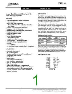
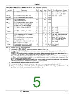
X96010
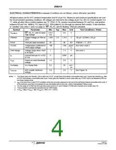
D/A CONVERTER CHARACTERISTICS (See pg. 4 for Standard Conditions)
Symbol
IFS
Parameter
Min Typ
Max
1.6
3.2
1
Unit
mA
Test Conditions / Notes
See note 1, 5, R = 510Ω
See note 1, 4, 6, R = 255Ω
I1 or I2 full scale current
1.56 1.58
mA
OffsetDAC
FSErrorDAC
DNLDAC
I1 or I2 D/A converter offset error
I1 or I2 D/A converter full scale error
1
-2
LSB See notes 2 and 3.
2
LSB
LSB
I1 or I2 D/A converter
Differential Nonlinearity
-0.5
0.5
INLDAC
I1 or I2 D/A converter Integral Nonlin-
earity with respect to a straight line
through 0 and the full scale value
-1
1
LSB
VISink
I1 or I2 Sink Voltage Compliance
1.2
2.5
0
Vcc
Vcc
V
V
See note 5
See note 4, 6
See note 5
VISource
I1 or I2 Source Voltage Compliance
Vcc-1.2
Vcc-2.5
0
V
0
V
See note 4, 6
IOVER
I1 or I2 overshoot on D/A Converter
data byte transition
µA
DAC input byte changing from
00h to FFh and vice
versa, V(I1) and V(I2) are
Vcc - 1.2V in source mode
and 1.2V in sink mode.
IUNDER
trDAC
I1 or I2 undershoot on D/A Converter
data byte transition
0
µA
µs
I1 or I2 rise time on D/A Converter data
byte transition; 10% to 90%
5
30
See note 4.
TCOIout
Temperataure coefficient of output
current due to internal parameters
-100
+100
ppm/ See Figure 7.
°C VRMbit = “0”
Notes: 1. DAC input Byte = FFh, Source or sink mode.
2
3
V(VRef)
255
2. LSB is defined as
divided by the resistance between R1 or R2 to Vss.
x
[
]
3. OffsetDAC: The Offset of a DAC is defined as the deviation between the measured and ideal output, when the DAC input is 01h. It is
expressed in LSB.
FSErrorDAC: The Full Scale Error of a DAC is defined as the deviation between the measured and ideal output, when the input is FFh. It
is expressed in LSB. The OffsetDAC is subtracted from the measured value before calculating FSErrorDAC
.
DNLDAC: The Differential Non-Linearity of a DAC is defined as the deviation between the measured and ideal incremental change in
the output of the DAC, when the input changes by one code step. It is expressed in LSB. The measured values are adjusted for Offset
and Full Scale Error before calculating DNLDAC
.
INLDAC: The Integral Non-Linearity of a DAC is defined as the deviation between the measured and ideal transfer curves, after adjust-
ing the measured transfer curve for Offset and Full Scale Error. It is expressed in LSB.
4. These parameters are periodically sampled and not 100% tested.
5. V(I1) and V(I2) are VCC - 1.2V in source mode and 1.2V in sink mode. In this range the current at I1 or I2 varies <1%.
6. The maximum current, sink or source, can be set with an external resistor to 3.2 mA with a minimum VCC = 4.5V. The compliance volt-
age changes to 2.5V from the sourcing rail, and the current variation is <1%.
FN8214.1
5
October 25, 2005

 INTERSIL [ Intersil ]