X96010
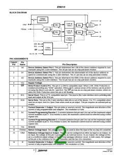
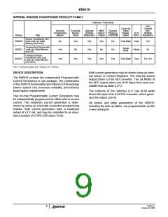
BLOCK DIAGRAM
Voltage
Reference
R2
I2
Look-up
Table 2
VRef
Mux
DAC 2
DAC 1
Mux
Mux
ADC
VSense
Look-up
Table 1
Mux
I1
R1
Control
& Status
SDA
SCL
2-Wire
Interface
WP
A2, A1, A0
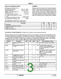
PIN ASSIGNMENTS
TSSOP
Pin
Pin
Name
Pin Description
1
2
3
A0
A1
A2
Device Address Select Pin 0. This pin determines the LSB of the device address required to com-
municate using the 2-wire interface. The A0 pin has an on-chip pull-down resistor.
Device Address Select Pin 1. This pin determines the intermediate bit of the device address re-
quired to communicate using the 2-wire interface. The A1 pin has an on-chip pull-down resistor.
Device Address Select Pin 2. This pin determines the MSB of the device address required to com-
municate using the 2-wire interface. The A2 pin has an on-chip pull-down resistor.
4
5
Vcc
WP
Supply Voltage.
Write Protect Control Pin. This pin is a CMOS compatible input. When LOW, Write Protection is
enabled preventing any “Write” operation. When HIGH, various areas of the memory can be protect-
ed using the Block Lock bits BL1 and BL0. The WP pin has an on-chip pull-down resistor, which en-
ables the Write Protection when this pin is left floating.
6
7
SCL
SDA
Serial Clock. This is a TTL compatible input pin. This input is the 2-wire interface clock controlling data
input and output at the SDA pin.
Serial Data. This pin is the 2-wire interface data into or out of the device. It is TTL compatible when
used as an input, and it is Open Drain when used as an output. This pin requires an external pull up
resistor.
8
9
I1
Current Generator 1 Output. This pin sinks or sources current. The magnitude and direction of the
current is fully programmable and adaptive. The resolution is 8 bits.
R1
Current Programming Resistor 1. A resistor between this pin and Vss can set the maximum output
current available at pin I1. If no resistor is used, the maximum current must be selected using control
register bits.
10
R2
Current Programming Resistor 2. A resistor between this pin and Vss can set the maximum output
current available at pin I2. If no resistor is used, the maximum current must be selected using control
register bits.
11
12
13
Vss
Ground.
VSense Sensor Voltage Input. This voltage input may be used to drive the input of the on-chip A/D converter.
VRef
Reference Voltage Input or Output. This pin can be configured as either an Input or an Output. As
an Input, the voltage at this pin is provided by an external source. As an Output, the voltage at this
pin is a buffered output voltage of the on-chip bandgap reference circuit. In both cases, the voltage
at this pin is the reference for the A/D converter and the two D/A converters.
14
I2
Current Generator 2 Output. This pin sinks or sources current. The magnitude and direction of the
current is fully programmable and adaptive. The resolution is 8 bits.
FN8214.1
October 25, 2005
2

 INTERSIL [ Intersil ]