X96010
X96010 Memory Map
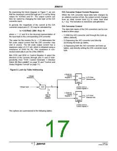
Addressing Protocol Overview
The X96010 contains a 144 byte array of mixed vola-
tile and nonvolatile memory. This array is split up into
three distinct parts, namely: (Refer to figure 14.)
All Serial Interface operations must begin with a
START, followed by a Slave Address Byte. The Slave
address selects the X96010, and specifies if a Read or
Write operation is to be performed.
– Look-up Table 1 (LUT1)
– Look-up Table 2 (LUT2)
– Control and Status Registers
It should be noted that the Write Enable Latch (WEL)
bit must first be set in order to perform a Write opera-
tion to any other bit. (See “WEL: Write Enable Latch
(Volatile)” on page 13.) Also, all communication to the
X96010 over the 2-wire serial bus is conducted by
sending the MSB of each byte of data first.
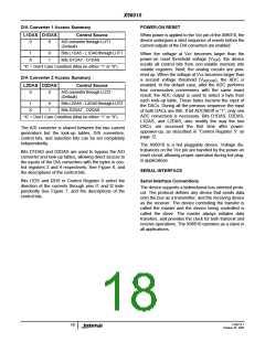
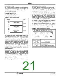
Figure 14. X96010 Memory Map
Address
Size
The memory is physically realized as one contiguous
array, organized as 9 pages of 16 bytes each.
10Fh
FFh
Look-up Table 2
(LUT2)
64 Bytes
64 Bytes
16 Bytes
The X96010 2-wire protocol provides one address
byte, therefore the next few sections explain how to
access the different areas for reading and writing.
D0h
CFh
Look-up Table 1
(LUT1)
90h
8Fh
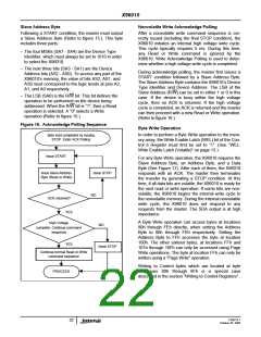
Figure 15. Slave Address (SA) Format
Control & Status
Registers
SA7 SA6
SA3 SA2
SA5 SA4
SA1
SA0
80h
1
0
1
0
AS2 AS1 AS0 R/W
The Control and Status registers of the X96010 are
used in the test and setup of the device in a system.
These registers are realized as a combination of both
volatile and nonvolatile memory. These registers
reside in the memory locations 80h through 8Fh. The
reserved bits within registers 80h through 86h, must
be written as “0” if writing to them, and should be
ignored when reading. Register bits shown as 0 or 1,
in Figure 4, must be written with the indicated value if
writing to them. The reserved registers, from 88h
through 8Fh, must not be written, and their content
should be ignored.
Device Type
Identifier
Device
Read or
Write
Address
Slave Address
Bit(s)
Description
SA7 - SA4
SA3 - SA1
SA0
Device Type Identifier
Device Address
Read or Write Operation Select
Both look-up tables LUT1 and LUT2 are realized as
nonvolatile EEPROM, and extend from memory loca-
tions 90h - CFh and D0h - 10Fh respectively. These
look-up tables are dedicated to storing data solely for
the purpose of setting the outputs of Current Genera-
tors I1 and I2 respectively.
All bits in both look-up tables are preprogrammed to
“0” at the factory.
FN8214.1
October 25, 2005
21

 INTERSIL [ Intersil ]