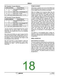
X96010
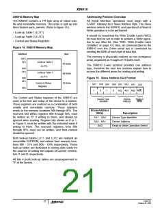
Figure 21. Read Sequence
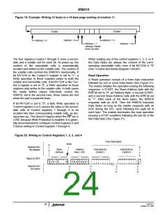
S
t
a
r
S
Slave
Address
with
Slave
Address
with
Signals
from the
Master
S
t
o
p
t
a
r
A
C
K
A
C
K
Address
Byte
R/W = 0
R/W = 1
t
t
Signal at
SDA
10 1 0
10 1 0
1
0
A
C
K
A
C
K
A
C
K
Signals from
the Slave
Last Read
Data Byte
First Read
Data Byte
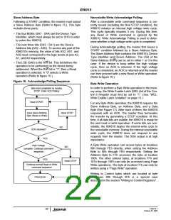
The Data Bytes are from the memory location indicated
by an internal pointer. This pointer initial value is deter-
mined by the Address Byte in the Read operation instruc-
tion, and increments by one during transmission of each
Data Byte. After reaching the memory location 10Fh, a
stop should be issued.
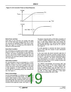
Data Protection
There are three levels of data protection designed into
the X96010: 1- Any Write to the device first requires
setting of the WEL bit in Control 6 register; 2- The
Write Protection pin disables any writing to the
X96010; 3- The proper clock count, data bit sequence,
and STOP condition is required in order to start a nonvol-
atile write cycle, otherwise the X96010 ignores the Write
operation.
If the read operation continues, the output bytes are
unpredictable. If the address is set between 00h and
7Fh, the output bytes are unpredictable.
A Read operation internal pointer can start at any
memory location from 80h through FEh, when the
Address Byte is 80h through FEh respectively. But it
starts at location 100h if the Address Byte is FFh.
WP: Write Protection Pin
When the Write Protection (WP) pin is active (LOW),
any Write operations to the X96010 is disabled, except
the writing of the WEL bit.
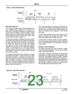
When reading any of the control registers 1, 2, 3, or 4,
the Data Bytes are always the content of the corre-
sponding nonvolatile cells, even if bit NV1234 is "0"
(See “Control and Status Register Format”).
FN8214.1
25
October 25, 2005

 INTERSIL [ Intersil ]