X96010
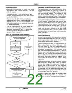
Figure 19. Example: Writing 12 bytes to a 16-byte page starting at location 11.
5 b5ybtyetess
7 bytes
Address = 6
Address = 11
Address = 0
Address = 7
Address = 15
Address Pointer
Ends Up Here
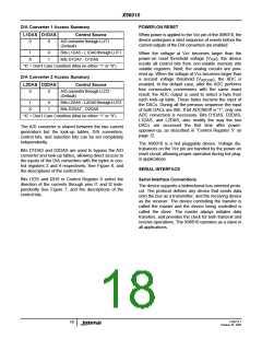
The four registers Control 1 through 4, have a nonvol-
atile and a volatile cell for each bit. At power-up, the
content of the nonvolatile cells is automatically
recalled and written to the volatile cells. The content of
the volatile cells controls the X96010’s functionality. If
bit NV1234 in the Control 0 register is set to “1”, a
Write operation to these registers writes to both the
volatile and nonvolatile cells. If bit NV1234 in the Con-
trol 0 register is set to “0”, a Write operation to these
registers only writes to the volatile cells. In both cases
the newly written values effectively control the
X96010, but in the second case, those values are lost
when the part is powered down.
When reading any of the control registers 1, 2, 3, or 4,
the Data Bytes are always the content of the corre-
sponding nonvolatile cells, even if bit NV1234 is "0"
(See “Control and Status Register Format”).
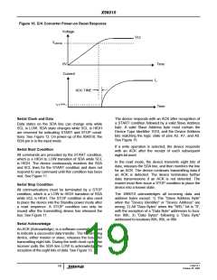
Read Operation
A Read operation consist of a three byte instruction
followed by one or more Data Bytes (See Figure 21).
The master initiates the operation issuing the following
sequence: a START, the Slave Address byte with the
R/W bit set to “0”, an Address Byte, a second START,
and a second Slave Address byte with the R/W bit set
to “1”. After each of the three bytes, the X96010
responds with an ACK. Then the X96010 transmits
Data Bytes as long as the master responds with an
ACK during the SCL cycle following the eigth bit of
each byte. The master terminates the read operation
(issuing a STOP condition) following the last bit of the
last Data Byte (See Figure 21).
If bit NV1234 is set to “0”, a Byte Write operation to
Control registers 0 or 5 causes the value in the nonvol-
atile cells of Control registers 1 through 4 to be
recalled into their corresponding volatile cells, as dur-
ing power-up. This doesn’t happen when the WP pin is
LOW, because Write Protection is enabled. It is gener-
ally recommended to configure Control registers 0 and
5 before writing to Control registers 1 through 4.
Figure 20. Writing to Control Registers 1, 2, 3, and 4
Four Data Bytes
Write
S
Signals from
the Master
S
t
o
p
t
a
r
Slave
Address
Address
Byte = 81h
Data Byte for
Control 1
Data Byte for
Control 4
t
Signal at SDA
10 1 0
0
10 0 0
0 0 01
Signals from
the Slave
A
C
K
A
C
K
A
C
K
A
C
K
FN8214.1
24
October 25, 2005

 INTERSIL [ Intersil ]