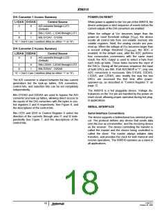
X96010
Slave Address Byte
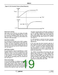
Nonvolatile Write Acknowledge Polling
Following a START condition, the master must output
a Slave Address Byte (Refer to figure 15.). This byte
includes three parts:
After a nonvolatile write command sequence is cor-
rectly issued (including the final STOP condition), the
X96010 initiates an internal high voltage write cycle.
This cycle typically requires 5 ms. During this time,
any Read or Write command is ignored by the
X96010. Write Acknowledge Polling is used to deter-
mine whether a high voltage write cycle is completed.
– The four MSBs (SA7 - SA4) are the Device Type
Identifier, which must always be set to 1010 in order
to select the X96010.
– The next three bits (SA3 - SA1) are the Device
Address bits (AS2 - AS0). To access any part of the
X96010’s memory, the value of bits AS2, AS1, and
AS0 must correspond to the logic levels at pins A2,
A1, and A0 respectively.
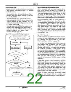
During acknowledge polling, the master first issues a
START condition followed by a Slave Address Byte.
The Slave Address Byte contains the X96010’s Device
Type Identifier and Device Address. The LSB of the
Slave Address (R/W) can be set to either 1 or 0 in this
case. If the device is busy within the high voltage
cycle, then no ACK is returned. If the high voltage
cycle is completed, an ACK is returned and the master
can then proceed with a new Read or Write operation.
(Refer to figure 16.).
– The LSB (SA0) is the R/W bit. This bit defines the
operation to be performed on the device being
addressed. When the R/W bit is “1”, then a Read
operation is selected. A “0” selects a Write
operation (Refer to figure 15.)
Figure 16. Acknowledge Polling Sequence
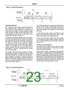
Byte Write Operation
In order to perform a Byte Write operation to the mem-
ory array, the Write Enable Latch (WEL) bit of the Con-
trol 6 Register must first be set to “1”. (See “WEL:
Write Enable Latch (Volatile)” on page 13.)
Byte load completed by issuing
STOP. Enter ACK Polling
Issue START
For any Byte Write operation, the X96010 requires the
Slave Address Byte, an Address Byte, and a Data
Byte (See Figure 17). After each of them, the X96010
responds with an ACK. The master then terminates
the transfer by generating a STOP condition. At this
time, if all data bits are volatile, the X96010 is ready for
the next read or write operation. If some bits are non-
volatile, the X96010 begins the internal write cycle to
the nonvolatile memory. During the internal nonvolatile
write cycle, the X96010 does not respond to any
requests from the master. The SDA output is at high
impedance.
Issue STOP
Issue Slave Address
Byte (Read or Write)
NO
ACK returned?
YES
A Byte Write operation can access bytes at locations
80h through FEh directly, when setting the Address
Byte to 80h through FEh respectively. Setting the
Address Byte to FFh accesses the byte at location
100h. The other sixteen bytes, at locations FFh and
101h through 10Fh can only be accessed using Page
Write operations. The byte at location FFh can only be
written using a “Page Write” operation.
High Voltage
complete. Continue command
sequence.
NO
YES
Issue STOP
Continue normal Read or Write
command sequence
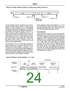
Writing to Control bytes which are located at byte
addresses 80h through 8Fh is a special case
described in the section “Writing to Control Registers” .
PROCEED
FN8214.1
22
October 25, 2005

 INTERSIL [ Intersil ]