X5043, X5045
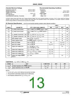
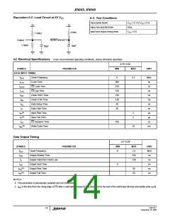
Equivalent A.C. Load Circuit at 5V V
A.C. Test Conditions
CC
Input pulse levels
VCC x 0.1 to VCC x 0.9
10ns
5V
5V
Input rise and fall times
Input and output timing level
V
CC x 0.5
4.6kΩ
1.64kΩ
Output
1.64kΩ
RESET/RESET
30pF
30pF
AC Electrical Specifications (Over recommended operating conditions, unless otherwise specified)
2.7V–5.5V
SYMBOL
PARAMETER
MIN
MAX
UNIT
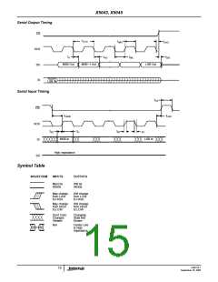
DATA INPUT TIMING
fSCK
tCYC
tLEAD
tLAG
tWH
tWL
Clock Frequency
0
3.3
MHz
ns
Cycle Time
300
150
150
130
130
30
CS Lead Time
CS Lag Time
ns
ns
Clock HIGH Time
Clock LOW Time
Data Setup Time
Data Hold Time
Input Rise Time
Input Fall Time
CS Deselect Time
Write Cycle Time
ns
ns
tSU
ns
tH
30
ns
(4)
tRI
2
2
µs
µs
ns
(4)
tFI
tCS
100
(5)
tWC
10
ms
Data Output Timing
2.7–5.5V
SYMBOL
PARAMETER
MIN
MAX
3.3
UNIT
MHz
ns
fSCK
tDIS
tV
Clock Frequency
0
Output Disable Time
Output Valid from Clock Low
Output Hold Time
150
120
ns
tHO
0
ns
(4)
tRO
Output Rise Time
50
50
ns
(4)
tFO
Output Fall Time
ns
NOTES:
4. This parameter is periodically sampled and not 100% tested.
5. tWC is the time from the rising edge of CS after a valid write sequence has been sent to the end of the self-timed internal nonvolatile write cycle.
FN8126.1
14
September 16, 2005

 INTERSIL [ Intersil ]