ISL6366
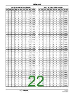
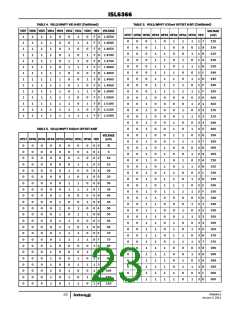
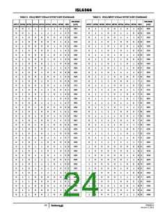
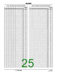
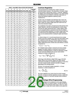
TABLE 5. VR12/IMVP7 635mV OFFSET 8-BIT (Continued)
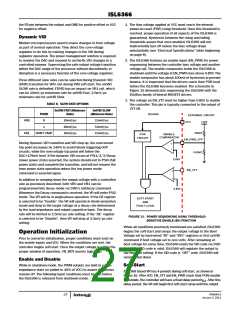
Load-Line Regulation
VOLTAGE
Some microprocessor manufacturers require a precisely
controlled output resistance. This dependence of output voltage
on load current is often termed “droop” or “load line” regulation.
By adding a well controlled output impedance, the output voltage
can effectively be level shifted in a direction, which works to
achieve the load-line regulation required by these
manufacturers.
OFS7 OFS6 OFS5 OFS4 OFS3 OFS2 OFS1 OFS0 HEX
(mV)
-190
-185
-180
-175
-170
-165
-160
-155
-150
-145
-140
-135
-130
-125
-120
-115
-110
-105
-100
-95
1
1
1
1
1
1
1
1
1
1
1
1
1
1
1
1
1
1
1
1
1
1
1
1
1
1
1
1
1
1
1
1
1
1
1
1
1
1
1
1
1
1
1
1
1
1
1
1
1
1
1
1
1
1
1
1
1
1
1
1
1
1
1
1
1
1
1
1
1
1
1
1
1
1
1
1
0
0
0
0
0
0
1
1
1
1
1
1
1
1
1
1
1
1
1
1
1
1
1
1
1
1
1
1
1
1
1
1
1
1
1
1
1
1
1
1
1
1
1
1
0
0
0
0
0
0
0
0
0
0
0
0
0
0
0
0
1
1
1
1
1
1
1
1
1
1
1
1
1
1
1
1
1
1
1
1
1
1
0
0
0
0
0
0
0
0
1
1
1
1
1
1
1
1
0
0
0
0
0
0
0
0
1
1
1
1
1
1
1
1
0
0
1
1
1
1
0
0
0
0
1
1
1
1
0
0
0
0
1
1
1
1
0
0
0
0
1
1
1
1
0
0
0
0
1
1
1
1
1
1
0
0
1
1
0
0
1
1
0
0
1
1
0
0
1
1
0
0
1
1
0
0
1
1
0
0
1
1
0
0
1
1
0
0
1
1
0
1
0
1
0
1
0
1
0
1
0
1
0
1
0
1
0
1
0
1
0
1
0
1
0
1
0
1
0
1
0
1
0
1
0
1
0
1
D
D
D
D
D
D
E
E
E
E
E
E
E
E
E
E
E
E
E
E
E
E
F
F
F
F
F
F
F
F
F
F
F
F
F
F
F
F
A
B
C
D
E
F
In other cases, the designer may determine that a more cost-
effective solution can be achieved by adding droop. Droop can
help to reduce the output-voltage spike that results from fast
load-current demand changes.
0
1
2
3
4
5
6
7
8
9
A
B
C
D
E
F
The magnitude of the spike is dictated by the ESR and ESL of the
output capacitors selected. By positioning the no-load voltage
level near the upper specification limit, a larger negative spike
can be sustained without crossing the lower limit. By adding a
well controlled output impedance, the output voltage under load
can effectively be level shifted down so that a larger positive
spike can be sustained without crossing the upper specification
limit.
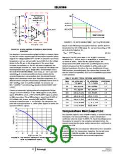
As shown in Figure 14, a current proportional to the average
current of all active channels, I
, flows from FB through a load-
AVG
line regulation resistor R . The resulting voltage drop across
FB
R
is proportional to the output current, effectively creating an
FB
output voltage droop with a steady-state value defined, as shown
in Equation 13:
V
= I
⋅ R
AVG
FB
(EQ. 13)
DROOP
The regulated output voltage is reduced by the droop voltage
. The output voltage as a function of load current is
V
DROOP
derived by combining Equation 13 with the appropriate sample
current expression defined by the current sense method
employed, as shown in Equation 14:
-90
-85
I
R
⎛
⎞
⎟
LOAD
N
X
0
1
2
3
4
5
6
7
8
9
A
B
C
D
E
F
-80
(EQ. 14)
V
= V
– --------------- ----------------- R
⎜
REF FB
OUT
R
ISEN
⎝
⎠
-75
where V
is the reference voltage (DAC), I
is the total
is the sense resistor
-70
REF
output current of the converter, R
LOAD
ISEN
-65
connected to the ISEN+ pin, and R is the feedback resistor, N is
FB
the active channel number, and R is the DCR, or R
-60
X
SENSE
depending on the sensing method.
-55
Therefore, the equivalent loadline impedance, i.e. Droop
impedance, is equal to Equation 15:
-50
-45
R
R
X
R
ISEN
FB
R
= ------------ -----------------
(EQ. 15)
LL
-40
N
-35
The major regulation error comes from the current sensing
elements. To improve load-line regulation accuracy, a tight DCR
tolerance of inductor or a precision sensing resistor should be
considered.
-30
-25
-20
Output-Voltage Offset Programming
-15
The output voltage can be margined in ±5mV steps between
-640mV and 635mV, as shown in Table 5, via SVID set OFFSET
command (33h). The minimum offset step is ±5mV. For a finer
than 5mV offset, a large ratio resistor divider can be placed on
-10
-5
FN6964.0
January 3, 2011
26

 INTERSIL [ Intersil ]