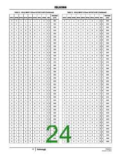
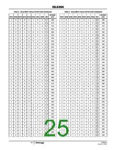
ISL6366
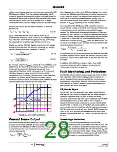
voltage reaches V
BOOT
voltage at a fixed slew rate, quarter of setVID
where V
is the voltage at the IMON pin, R
is the resistor
IMON
IMON
is the total output current
FAST rate as in Table 6. Then, the controller will regulate the VR
voltage at V for another period t until SVID sends a new VID
between the IMON pin and GND, I
of the converter, R
LOAD
is the sense resistor connected to the
ISEN
BOOT D3
command. If the VID code is valid, ISL6366 will initiate the second
soft-start ramp at a slew rate, set by SetDVID FAST or SLOW
command in Table 6, until the voltage reaches the new VID voltage.
ISEN+ pin, N is the active channel number, and R is the DC
resistance of the current sense element, either the DCR of the
X
inductor or R
depending on the sensing method.
SENSE
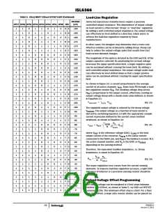
The resistor from the IMON pin to GND should be chosen to
ensure that the voltage at the IMON pin is typically 900mV at the
The soft-start time is the sum of the 4 periods, as shown in
Equation 16.
maximum load current, typically corresponding to I
CCMAX
t
= t + t + t + t
D1 D2 D3 D4
(EQ. 16)
SS
register. The IMON voltage is linearly digitized every 132µs and
stored in the IOUT register (15h). When the IMON voltage reaches
900mV or beyond, the digitized IOUT will be FFh and the Alert pin
is pulled low to alarm the CPU. If the desired maximum load
t
is a fixed delay with the typical value as 4.6ms. t is
D3
D1
determined by the time to obtain a valid new VID voltage from SVID
bus. If the VID is valid before the output reaches the boot voltage,
the output will turn around to respond to the new VID code.
current alert is not the exact I
value, the IMON resistor can
CCMAX
be scaled accordingly to make sure that it reaches 900mV at the
desired maximum output load.I
During t and t , ISL6366 digitally controls the DAC voltage
D2 D4
0.9V R
change at 5mV per step. The soft-start ramp time t and t
D2
D4
N
ISEN
(EQ. 20)
R
= ----------------------------- --------------------------------------
IMON
can be calculated based on Equations 17 and 18:
R
I
DESIRED_MAX
X
V
BOOT
---------------------------------------------------
t
=
(μs)
A small capacitor can be placed between the IMON pin and GND
to reduce the noise impact and do the average. The typical time
constant is 1ms for VR12 applications. If this pin is not used, tie
it to GND.
(EQ. 17)
(EQ. 18)
D2
SetVID SLOW RATE
V
– V
VID
BOOT
-----------------------------------
t
=
(μs)
D4
SetVID RATE
In addition, if the IMON pin voltage is higher than 1.12V,
overcurrent shutdown will be triggered, as described in
“Overcurrent Protection” on page 29.
For example, when the V
BOOT
at 10mV/µs, the first soft-start ramp time t will be around
440µs and the second soft-start ramp time t will be at
D4
is set at 1.1V and setVID rate is set
D2
maximum of 40µs if an setVID command for 1.5V is received
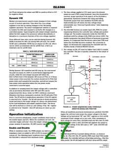
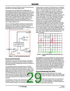
Fault Monitoring and Protection
after t . However, if V
is set at 0V, the first setVID
D3 BOOT
The ISL6366 actively monitors output voltage and current to detect
fault conditions. Fault monitors trigger protective measures to
prevent damage to a microprocessor load. One common power-
good indicator is provided for linking to external system monitors.
The schematic in Figure 17 outlines the interaction between the
fault monitors and the VR_RDY signal.
command is for 1.5V, then t will be around 150µs. Note that
D2
the initial 0 to 250mV DAC is typically at a slower rate to
minimize the inrush current, the response time could be dictated
by the compensation network and the output filter.
VR_Ready Signal
The VR_RDY pin is an open-drain logic output which indicates
that the soft-start period is complete and the output voltage is
within the regulated range. VR_RDY is pulled low during
shutdown and releases high after a successful soft-start. VR_RDY
will be pulled low when an fault (OCP or OVP) condition is
detected, or the controller is disabled by a reset from EN_PWR,
EN_VTT, POR, or VID OFF-code. If the Multi_VR_config register is
set to 01h, then the VR_Ready line will stay high when receiving a
00h VID code after the first soft-start. The VR_RDYS behaves the
same as VR_RDY, and both are independent from each other.
However, the defaulted Multi_VR_config is 00h for VR0 and 01h
for VR1.
t
t
D3
t
t
D2
D1
D4
EN_VTT
VR_Ready
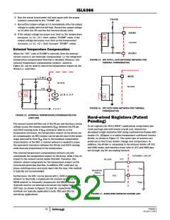
FIGURE 16. SOFT-START WAVEFORMS
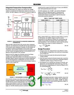
Current Sense Output
Overvoltage Protection
Regardless of the VR being enabled or not, the ISL6366
overvoltage protection (OVP) circuit will be active after its POR. The
OVP thresholds are different under different operation conditions.
When VR is not enabled and during the soft-start intervals t , the
OVP threshold is 2.3V. Once the VR output voltage reaches above
the DAC, fires the first PWM and completes the soft-start, the OVP
trip point will change to a tacking level of DAC+179mV.
The current flowing out of the IMON pin is equal to the sensed
average current inside ISL6366. In typical applications, a resistor
is placed from the IMON pin to GND to generate a voltage, which
is proportional to the load current and the resistor value, as
shown in Equation 19:
D1
R
R
IMON
X
(EQ. 19)
V
= ------------------ -----------------I
LOAD
IMON
N
R
ISEN
FN6964.0
January 3, 2011
28

 INTERSIL [ Intersil ]