ISL6366
the FB pin between the output and GND for positive offset or VCC
for negative offset.
1. The bias voltage applied at VCC must reach the internal
power-on reset (POR) rising threshold. Once this threshold is
reached, proper operation of all aspects of the ISL6366 is
guaranteed. Hysteresis between the rising and falling
thresholds assure that once enabled, ISL6366 will not
inadvertently turn off unless the bias voltage drops
substantially (see “Electrical Specifications” table beginning
on page 8).
Dynamic VID
Modern microprocessors need to make changes to their voltage
as part of normal operation. They direct the core-voltage
regulator to do this by making changes to the VID during
regulator operation. The power management solution is required
to monitor the DAC and respond to on-the-fly VID changes in a
controlled manner. Supervising the safe output voltage transition
within the DAC range of the processor without discontinuity or
disruption is a necessary function of the core-voltage regulator.
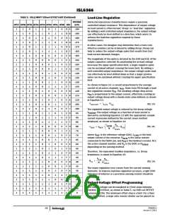
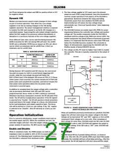
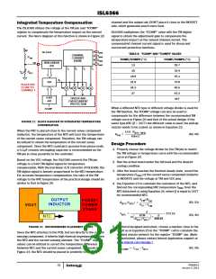
2. The ISL6366 features an enable input (EN_PWR) for power
sequencing between the controller bias voltage and another
voltage rail. The enable comparator holds the ISL6366 in
shutdown until the voltage at EN_PWR rises above 0.85V. The
enable comparator has about 100mV of hysteresis to prevent
bounce. It is important that the drivers reach their POR level
before the ISL6366 becomes enabled. The schematic in
Figure 15 demonstrates sequencing the ISL6366 with the
ISL66xx family of Intersil MOSFET drivers.
Three different slew rates can be selected during Dynamic VID
(DVID) transition for VR0, but during VR0 soft-start, the setVID
SLOW rate is defaulted. FDVID has no impact on VR1 rail, which
can be 10mV/µs minimum rate for setVID Fast, 2.5mV/µs
minimum rate for setVID Slow.
3. The voltage on EN_VTT must be higher than 0.85V to enable
the controller. This pin is typically connected to the output of
VTT VR.
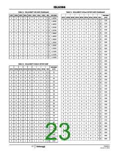
TABLE 6. SLEW RATE OPTIONS
SetVID FAST (Minimum
Rate)
SetVID SLOW
(Minimum Rate)
ISL6366
FDVID
EXTERNAL CIRCUIT
VR0
VR1
0
10mV/µs
20mV/µs
10mV/µs
2.5mV/µs
5.0mV/µs
2.5mV/µs
VCC
+12V
1
DON’T CARE
100kΩ
POR
ENABLE
COMPARATOR
CIRCUIT
EN_PWR_CFP
During dynamic VID transition and VID step up, the overcurrent
trip point increases by 140% to avoid falsely triggering OCP
circuits, while the overvoltage trip point will follow the
DAC+179mV level. If the dynamic VID occurs at PSI1/2/3/Decay
(lower power state) asserted, the system should exit to PSI0 (full
power state) and complete the transition, and will not resume the
lowe power state operation unless the low power mode
command is asserted again.
+
-
9.09kΩ
0.85V
EN_VTT
+
-
In addition to ramping down the output voltage with a controlled
rate as previously described, both VR0 and VR1 can be
programmed into decay mode via SVID’s setDecay command.
Whenever the Decay command is received, the VR will enter PSI2
mode. The VR will be in single-phase operation. If the DE register
is selected to be “Enable”, the VR will operate in diode emulation
mode and drop to the target voltage at a decay rate determined
by the load impedance and output capacitive bank. The decay
rate will be limited to 2.5mV/µs rate setting. If the “DE” register
is selected to be “Disable”, then VR will drop at 2.5mV/µs rate
setting.
0.85V
SOFT-START
AND
FAULT LOGIC
FIGURE 15. POWER SEQUENCING USING THRESHOLD-
SENSITIVE ENABLE (EN) FUNCTION
When all conditions previously mentioned are satisfied, ISL6366
begins the soft-start and ramps the output voltage to the Boot
Voltage set by hard-wired “BT” and “BTS” registers or first setVID
command if boot voltage set to zero volts. After remaining at
boot voltage for some time, ISL6366 reads the VID code via SVID
bus. If the VID code is valid, ISL6366 will regulate the output to
the final VID setting. If the VID code is “OFF” code, ISL6366 will
remain shut down.
Operation Initialization
Prior to converter initialization, proper conditions must exist on
the enable inputs and VCC. When the conditions are met, the
controller begins soft-start. Once the output voltage is within the
proper window of operation, VR_RDY asserts logic high.
Enable and Disable
While in shutdown mode, the PWM outputs are held in a high-
impedance state (or pulled to 40% of VCC) to assure the drivers
remain off. The following input conditions must be met before
the ISL6366 is released from shutdown mode.
Soft-Start
ISL6366 based VR has 4 periods during soft-start, as shown in
Figure 16. After VCC, EN_VTT and EN_PWR reach their POR/enable
thresholds, the controller will have a fixed delay period t . After this
D1
delay period, the VR will begin first soft-start ramp until the output
FN6964.0
January 3, 2011
27

 INTERSIL [ Intersil ]