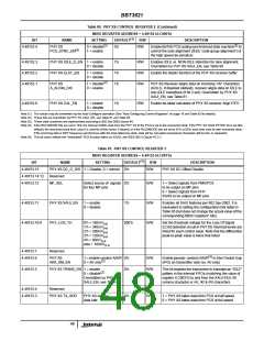
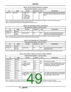
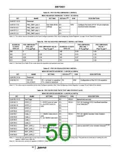
BBT3821
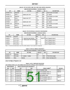
Table 92. AUTO-CONFIGURE REGISTERS (Continued)
Auto-configure Pointer is (S), Auto-configure Size is (N), from 1.8106’h & 1.8105’h respectively
(1)
NVR ADDRESS
DEC HEX
S + 7 S + 7
TARGET REGISTER BITS ADDRESS
DEC HEX
1.36865.[7:0] 1.9001.[7:0]
(1)
TARGET NAME
LASI TX Alarm Control
DETAILS
Table 25
S + 8
S + 8
1.36865.[10:8]
& 1.36866.[3:0]
1.9001.[10:8],
1.9002.[3:0]
LASI TX Alarm & LASI Control
Table 25 &
Table 26
S + 9
S + 9
S + A
S + B
1.36870.
1.36871.
1.9006
1.9007
DOM TX flag control
DOM RX flag control
Table 30
Table 31
S + 10
S + 11
1.49170.[1:0],
1.49168.[5:0]
1.C012.[1:0],
1.C010.[5:0]
GPIO LASI & Pin Direction Configuration
Table 49 &
Table 47
S + 12
S + 13
S + C
S + D
1.49170.[11:8,5:2],
1.C012.[11:8,5:2]
GPIO LASI control
Table 49
1.49170.[13:12],
1.49171.[5:0]
1.C012.[13:12],
1.C013.[5:0]
TX_FAULT polarity, GPIO LASI & Output Control Table 49 &
Table 50
S + 14
S + 15
S + 16
S + 17
S + 18
S + 19
S + 20
S + 21
S + 22
S + 23
S + 24
S + 25
S + 26
S + 27
S + 28
S + 29
S + 30
S + 31
S + 32
S + 33
S + 34
S + 35
S + 36
S + 37
S + E
1.49176
1.C018
DOM Control
Table 51
Table 53
S + F
1.49177.[7:0]
1.49177.[15:8]
1.49178.[7:0]
1.49178.[15:8]
1.49179.[7:0]
1.49179.[15:8]
1.49180.[7:0]
1.49180.[15:8]
1.49181.[7:0]
4.49152.[7:0]
4.49152.[15:8]
4.49153.[7:0]
4.49153.[15:8]
4.49154.[7:0]
4.49155.[7:0]
4.49156.[11:8,3:0]
3.49152.[7:0]
3.49152.[15:8]
3.49153.[7:0]
1:3.49153.[15:8]
3.49154.[7:0]
3.49155.[7:0]
1.C019.[7:0]
1.C019.[15:8]
1.C01A.[7:0]
1.C01A.[15:8]
1.C01B.[7:0]
1.C01B.[15:8]
1.C01C.[7:0]
1.C01C.[15:8]
1.C01D.[7:0]
4.C000.[7:0]
4.C000.[15:8]
4.C001.[7:0]
4.C001.[15:8]
4.C002.[7:0]
4.C003.[7:0]
4.C004.[11:8,3:0]
3.C000.[7:0]
3.C000.[15:8]
3.C001.[7:0]
1:3.C001.[15:8]
3.C002.[7:0]
3.C003.[7:0]
Indirect DOM Mem Address Lane2
Indirect DOM Mem Address Lane3
Indirect DOM Mem Address Lane0
Indirect DOM Mem Address Lane1
Indirect DOM Dev Address Lane2
Indirect DOM Dev Address Lane3
Indirect DOM Dev Address Lane0
Indirect DOM Dev Address Lane1
Optical I/F Pin Polarity Control
PHY XS control 2
S + 10
S + 11
S + 12
S + 13
S + 14
S + 15
S + 16
S + 17
S + 18
S + 19
S + 1A
S + 1B
S + 1C
S + 1D
S + 1E
S + 1F
S + 20
S + 21
S + 22
S + 23
S + 24
S + 25
Table 54
Table 55
Table 80
PHY XS control 2
PHY XS control 3
Table 81
PHY XS control 3
PHY XS Error Code
Table 82
Table 83
Table 85
Table 63
PHY XS IDLE Code
PHY XS Loopback Control
PCS control 2
PCS control 2
PCS control 3
Table 64 &
Table 39
(2)
PCS control 3/PMA control 2
PCS Error Code
Table 66
Table 67
Table 40 &
Table 68
Table 45
Table 91
PCS IDLE Code
1.49156.[11:8]
3.49156.[3:0]
1.C004.[11:8]
3.C004.[3:0]
PCS/PMA Loopback Control
(3)
S + 38
S + 39
S + 26
S + 27
1.49163.[9:2]
4.49163.[9:2]
1.C00B.[9:2]
4.C00B.[9:2]
Miscellaneous Adjustments
BitBlitz Internal Test Control
Note (1): The 8 bits of the NVR register (7:0) are mapped to the listed bits of the target in order. Unused bits are always at the MSb (bit 7) end.
Note (2): The target register pair are overlapped, ignoring the ‘reserved’ bits in one where used bits occur in the same location in the other. Thus the mapping from the
NVR register is: 1.C001.[15:12], 3.C001.11, 1.C001.[10:8].
Note (3): The mapping from the NVR register is: 1.C004.[11:8], 3.C004.[3:0]
52

 INTERSIL [ Intersil ]