BBT3821
Serial Test Loopbacks (1.C004.12 & 4.C004.12)
MDIO Register Addressing
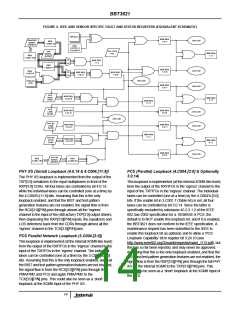
In addition to the above loopbacks, the BBT3821 also offers
two serial loopbacks directly between the serial inputs and
outputs. These loopbacks use the recovered clock as the
timing for the outputs (instead of the multiplied reference
clock), so do not reset the jitter or clock domains, and in
addition do NOT provide any pre-emphasis on the outputs.
Furthermore, on the PMA/PMD side (1.C004.12) the lanes
are internally swapped (so the Lane 3 output is from the
Lane 0 input, etc.). Because of their limited utility, they are
not illustrated in Figure 2 or Figure 6. They are mainly useful
for debugging an otherwise intractable system problem. The
reference clock still needs to be within locking range of the
input frequency. The remainder of the signal path will remain
active (as normal), so that if for example 1.C004.12 is set,
data coming in on RCX[3:0], in addition to emerging on
TCX[0:3] without retiming, etc., will also emerge from
TXP[3:0] retimed, as usual.
The PADR[4..0] hardware address pins control the PRTAD
(Port Address) value, each port normally consisting of a
series of MDIO Managed Devices (MMDs). Each Port may
include up to 31 different devices, of which the current
specification defines 8 types, and allows vendor
specification of two others. The BBT3821 device
corresponds to the PMA/PMD, PCS and PHY XGXS defined
types, so responds to DEVAD values of 1, 3 and 4
respectively. The Clause 45-accessible registers are listed
for each Device Address in the tables referenced in Table 2.
Many of these register addresses are IEEE-defined; the
‘Vendor Defined’ registers are arranged to be as DEVAD
independent as possible.
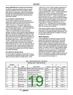
Table 2. DEVAD DEVICE ADDRESS TABLE
REGISTER LIST
DEVAD VALUE
IEEE DEFINITION
TABLE
DEVAD = 1 (00001’b) PMA/PMD Device
DEVAD = 3 (00011’b) PCS Device
Table 4, page 19
Table 56, page 38
Serial Management Interface
DEVAD = 4 (00100’b) PHY XS (XGXS) Device Table 74, page 45
The nLiten BBT3821 implements the MMD Management
Interface defined in IEEE 802.3-2002 Clauses 22 &
16
Each individual device may have up to 2 (65,536)
enhanced in IEEE 802.3ae-2002 Clause 45. This two-pin
interface allows serial read/write of the internal control
registers and consists of the MDC clock and MDIO data
terminals. The PADR[4..0] pins are used to select the ‘Port
address’ to which a given nLiten BBT3821 device responds.
The BBT3821 will ignore Clause 22 format frames (on a
frame-by-frame basis), based on the second ST (start) bit
value. The two formats are shown in Table 3, together with
the references to the respective IEEE 802.3 specifications.
registers. The BBT3821 implements all the defined registers
for 10GBASE PMA/PMD, 10GBASE-X PCS and PHY XS
devices, and a few Vendor Specific registers for each
DEVAD respectively. The latter have been placed in the
blocks beginning at D.C000’h so as to avoid the areas
currently defined as for use by the XENPAK module and
similar MSA devices, to facilitate use of the BBT3821 in such
modules and systems.
Table 3. MDIO MANAGEMENT FRAME FORMATS
CLAUSE 22 FORMAT (FROM TABLE 22-10 IN IEEE STD 802.3-2002 EDITION, FOR REFERENCE)
OPERN
Read
Write
PRE
1….1
ST
01
01
OP
10
01
PHYAD
PPPPP
PPPPP
REGAD
RRRRR
RRRRR
TA
Z0
10
DATA
DDDDDDDDDDDDDDDD
DDDDDDDDDDDDDDDD
IDLE
Z
Z
1….1
CLAUSE 45 FORMAT (FROM TABLE 45-64 IN IEEE 802.3.ae-2002)
OP PRTAD DEVAD TA ADDRESS/DATA
00 PPPPP DDDDD 10 AAAAAAAAAAAAAAAA
(1)
OPERN
PRE
1….1
1….1
1….1
1….1
ST
IDLE
Addrs
Write
00
00
00
00
Z
Z
Z
Z
(2)
01
11
10
PPPPP
PPPPP
PPPPP
DDDDD
DDDDD
DDDDD
10
Z0
Z0
DDDDDDDDDDDDDDDD
DDDDDDDDDDDDDDDD
DDDDDDDDDDDDDDDD
Read
Read Inc
Note (1): The ‘Preamble’ consists of at least 32 bits. After a software reset, a few extra preamble bits may be needed, depending on the MDC clock rate. See timing
diagrams in Figure 15 and Figure 17.
Note (2): The actual register will not be updated until up to three additional MDC cycles have been received. See Figure 15.
15

 INTERSIL [ Intersil ]