BBT3821
1.41216 (1.A100’h), so that one-time or (by default) periodic
updates of the DOM information can be loaded into the MDIO
DOM space by writing the appropriate values into it, as shown
in Table 38, page 33. The actual automatic update rates
selectable in this XENPAK-defined register are controlled by
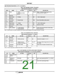
the DOM Control register in the BBT3821 vendor-specific
register space at 1.49176 (1.C018’h), which also controls other
actions of the DOM interface (see Table 51). In particular, since
many available DOM circuits can handle only one lane, bit 2
enables or disables indirect access to separate DOM circuits on
the four lanes. If the bit is 0’b, the DOM circuit is directly
addressed at Ax.00:FF’h, and is assumed to provide the full
four lane data, including the determination of which data is to be
treated as the ‘furthest out of range’ or the ‘representative
value’, as specified in Note 1 to Table 27 in section 11.2.6 of the
XENPAK R3.0 specification, to be returned in the XENPAK-
defined 1.A060:A06D’h space for a WDM module. If bit 2 of
1.C018’h is set to 1’b, the DOM data is polled from four devices
to the possible byte alignment and 8b/10b code violations,
which may be used to trigger a LASI. The available inputs
depend on the LX4/CX4 select LX4_MODE pin (Table 99),
and are detailed in Table 27 and Table 28, and include:
1. Various status bits within the BBT3821, derived from its
operations; in particular, the LOS indications, Byte Sync
and EFIFO errors, the Fault bits [1,3,4].8.10:11, etc.
2. The Optical Interface Status pins (in LX4 mode), see
Table 99.
3. The Alarm flags in 1.A070:1 (Table 36). These bits
are gated with the enable bits in 1.9006:7 (Table 30 and
Table 31) and the LX4/CX4 LX4_MODE pin (Table 99) to
drive bits 1.9004.1 & 1.9003.1 (Table 28 & Table 27).
4. The GPIO pins (Table 100). If configured as inputs, they
may be used to optionally trigger the LASI on either a
high or low level. See above.
These status inputs can all be read via the LASI Status
registers (1.9003 to 1.9005, see Table 27 to Table 29). Any of
these inputs, if enabled via the LASI Control Registers, 1.9000
to 1.9002 (Table 24 to Table 26), can drive the LASI pin.
2
attached to the I C serial bus, getting 10 bytes from each of
them. The 40 bytes of data are stored in the four lane register
blocks starting from 1.A0C0’h, 1.A0D0’h, 1.A0E0’h and
1.A0F0’h respectively. The device addresses of these four
DOM devices on the 2-wire bus are configured by registers
1.C01B’h and 1.C01C’h (Table 54); the starting memory
addresses by registers 1.C019’h and 1.C01A’h (Table 53).
Since the BBT3821 has no mechanism to determine out-of-
range data, it chooses one of these four 10-byte long groups of
data to copy into 1.A060’h:A069’h according to bits 1:0 of
1.C018’h (the ‘representative’ lane per the above-mentioned
XENPAK Note). In addition, the Alarm and Status flags
(Table 36 and Table 37) will be loaded from this lane into
1.A070:A075’h.
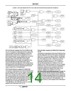
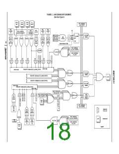
Figure 5 shows an equivalent schematic for the LASI system
(an expansion of Figure 21 in the XENPAK specification).
2
Reading Additional EEPROM Space Via the I C
Interface
2
The I C interface will allow single-byte reads from any
possible I C address. The device address and memory
2
address are written into the 1.32769 (1.8001’h) and
1.32770 (1.8002’h) registers respectively (see Table 16 and
Table 17), and on issuing a ‘Read one byte’ command (write
0002’h to 1.32768 = 1.8000’h) the data will be read from the
2
I C space in the MDIO register at 1.32771 (1.8003’h, see
The BBT3821 assumes that the DOM circuit(s) will have
these A/D values and flags at the same relative offsets as
those specified in the XENPAK R3.0 and the SFF-8472
specifications.
Table 18). For timing sequence, see Figure 22. Note that a
16-bit addressable EEPROM (or equivalent) device on the
2
I C bus may be read by setting the Long Memory bit
1.32773.8 (1.8005.8’h) to a ‘1’, and writing a full 16-bit
memory address value into 1.32770 (1.8002’h). This in
General Purpose (GPIO) Pins
2
principle allows access to almost a full 8MB of I C space,
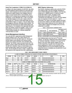
The BBT3821 includes some flexibly configurable General
Purpose Input-Output (GPIO) pins, which may be configured
to be inputs or outputs. As inputs, their level may be read
directly via the MDIO system, but also they may be
configured (again via MDIO registers, see Table 47 through
Table 50) to optionally trigger the LASI on either a high or
low level. The GPIO pins may also individually be used as
outputs, and set high or low, under MDIO control. The GPIO
control registers are among those that can be auto-
configured on start-up.
excluding only the NVR and (optional) DOM device address
portions. This 16-bit operation MUST NOT be used on an
8-bit device, since the register address setting operation will
attempt to write the low byte of the address into the register
at the high byte address. Such a 16-bit memory address
device should be located at a device address not used by
the NVR or DOM system.
These one-byte operations could be used to read other
types of data from (multiple) DOM devices (such as limit
lookup tables), or for expanded informational areas. It also
LASI Registers & I/O
2
facilitates the use of I C-based DCP (Digital Control
The BBT3821 implements the Link Alarm Status Interrupt
(LASI) interface defined in section 10.13 of the XENPAK
specification. The source and nature of these is described
above under “Error Indications” on page 13 and in Figure 4.
In addition to these specification-defined inputs, the
Potentiometer) devices for Laser Current control, and other
similar setup and monitoring uses.
BBT3821 incorporates a number of additional inputs, related
17

 INTERSIL [ Intersil ]