BBT3821
data is detected in all four lanes within the span of the
Alignment FIFO, the deskewing (lane to lane) alignment
operation is performed, and will be held until another ||A|| or
IDLE-to- non-IDLE transition is detected again on the lanes.
During this alignment, up to four code groups may be
deleted on any lane. For correct operation, the XAUI Lane 0
signals should be connected to the BBT3821 Lane 0 pins.
Transmitter Operations
8b/10b Encoding
The internal 10b encoding specified in the IEEE802.3-2002
specification, section 36.2.4 in Tables 36-1 & 36-2, and
discussed in more detail in “8b/10b Coding and Decoding”
page 12, is enabled by default in the PCS and PHY XS
through the setting of the respective CODECENA bits to 1’b,
and may be disabled through the MDIO registers
[3,4].C000’h (see Table 63 and Table 80) by setting the
respective bit to 0’b. Note that the receive decoding will also
be disabled. The (decoded, synchronized and aligned) data
is transferred via the transmit FIFOs, (normally) encoded,
serialized and re-transmitted on the Serial Output pins,
whose effective output impedance is nominally 100Ω
differential.
The deskew algorithm state machines (each implemented
according to IEEE 802.3ae) are enabled by setting the
DSKW_SM_EN bits (Address [3,4].C000’h, see Table 63
and/or Table 80) to 1 or overriding them with the respective
XAUI_EN bits in the [3,4].C001’h registers (Table 64 and
Table 81). Note that when one side’s DSKW_SM_EN is set
to 1, the same side CAL_EN bit (Address [3,4].C000’h,
Table 63/Table 80) is ignored. When a DSKW_SM_EN bit is
set to 0, lane deskew can still be enabled by setting
CAL_EN, but the deskew action will be carried out without
hysteresis.
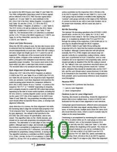
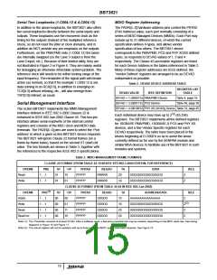
Pre-Emphasis
In order to compensate for the loss of the high frequency
signal component through PCB traces or the CX4 Cable
Assembly, sixteen levels of programmable pre-emphasis
have been provided on the CX4/LX4 PMA serial transmit
lanes, and eight levels on the XAUI PHY XS serial transmit
lanes. The output signal is boosted immediately after any
transition (see Figure 3). This maximizes the data eye
opening at the receiver inputs and enhances the bit error
rate performance of the system. The MDIO Registers at
Addresses [1,4].C005’h (see Table 41 and Table 85) control
the level of pre-emphasis for the PMA/PMD (sixteen levels)
and PHY XGXS (eight levels) respectively, settable from
none to the maximum. The initial default values of the
PMA/PMD register depend on the LX4_MODE configuration
pin, and are set to the optimum values for CX4 or XAUI
(assumed best for LX4 drivers). Both these registers may be
auto-loaded (see Auto-Configuring Control Registers
page 16) from an NVR EEPROM on start-up or RESET.
The user has the option to disable trunking, or to enable
trunking across each set of 4 lanes, in the PCS (device 3)
and PHY XGXS (device 4), under control of the respective
PSYNC bits in registers [3,4].C000h. In trunking mode, the
lanes may have phase differences, but they are expected to
be frequency synchronous. In non-trunking mode, each
received serial stream need only be within ±100ppm of the
nominal bit rate (2.488Gbps to 3.1875Gbps in full-speed
mode or 1.244Gbps to 1.59375Gbps in half-speed mode).
Setting the PSYNC bits high will enable the trunking mode,
so that all transmitted data will be synchronized to the same
clock. Note that trunking mode is only possible if 8B/10B
Coding is activated, and all lanes have the same half-rate
setting (See Table 71).
Clock Compensation
In addition to deskew, the Receive FIFOs also compensate
for clock differences. Since the received serial streams can,
under worst case conditions, be off by up to ±200ppm from
the local clock domain, the received data must be adjusted
to the local reference clock frequency.
FIGURE 3. PRE-EMPHASIS OUTPUT ILLUSTRATION
1
0
0
1
Another 8 bytes of RXFIFO are dedicated for clock
compensation. The FIFOs achieve clock tolerance by
identifying any of the IDLE patterns (/K/, /A/ or /R/ as defined
by the IEEE 802.3ae standard) in the received data and then
adding or dropping IDLEs as needed. The Receive FIFO
does not store the actual IDLE sequences received but
generates the number of IDLEs needed to compensate for
clock tolerance differences. The IDLE patterns retransmitted
will be determined according to the IEEE 802.3ae algorithm
if the appropriate AKR_SM_EN bit is set in Registers
[3,4].C001’h (see Table 64 and Table 81).
VLOW-pp
VHI-pp
Bit
Time
Bit
Time
Bit
Time
11

 INTERSIL [ Intersil ]