82C237
autoinitialize, even if the Mode register is programmed for lines to the latch. Address Enable (AEN) is used to enable
autoinitialization. An external EOP will autoinitialize the the bits onto the address bus through a three-state enable.
channel 1 registers, if so programmed. Data comparators in The lower order address bits are output by the 82C237
block search schemes may use the EOP input to terminate directly. Lines A0-A7 should be connected to the address
the service when a match is found. The timing of memory-to- bus. Figure 12 shows the time relationships between CLK,
memory transfers in found in Figure 13. Memory-to-memory AEN, ADSTB, DB0-DB7 and A0-A7.
operations can be detected as an active AEN with no DACK
During Block and Demand Transfer mode service, which
outputs.
include multiple transfers, the addresses generated will be
Priority - The 82C237 has two types of priority encoding sequential. For many transfers the data held in the external
available as software selectable options. The first is Fixed address latch will remain the same. This data need only
Priority which fixes the channels in priority order based upon change when a carry or borrow from A7 to A8 takes place in
the descending value of their numbers. The channel with the the normal sequence of addresses. To save time and speed
lowest priority is 3 followed by 2, 1 and the highest priority transfers, the 82C237 executes S1 states only when
channel, 0. After the recognition of any one channel for ser- updating of A8-A15 in the latch is necessary. This means for
vice, the other channels are prevented from interfering with long services, S1 states and Address Strobes may occur
the service until it is completed.
only once every 256 transfers, a savings of 255 clock cycles
for each 256 transfers.
The second scheme is Rotating Priority. The last channel to
get service becomes the lowest priority channel with the
others rotating accordingly. The next lower channel from the
channel serviced has highest priority on the following
request. Priority rotates every time control of the system
busses is returned to the processor.
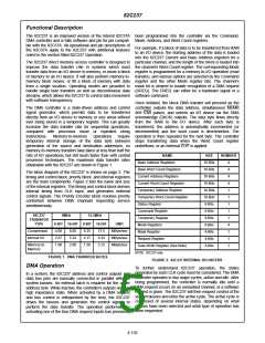
Programming
The 82C237 will accept programming from the host
processor anytime that HLDA is inactive, and at least one
rising CLK edge has occurred after HLDA went low. It is the
responsibility of the host to assure that programming and
HLDA are mutually exclusive.
Rotating Priority
1ST
2nd
3rd
SERVICE
SERVICE
SERVICE
Note that a problem can occur if a DMA request occurs on
an unmasked channel while the 82C237 is being pro-
grammed. For instance, the CPU may be starting to repro-
gram the two byte Address register of channel 1 when
channel 1 receives a DMA request. If the 82C237 is enabled
(bit 2 in the Command register is 0), and channel 1 is
unmasked, a DMA service will occur after only one byte of
the Address register has been reprogrammed. This condi-
tion can be avoided by disabling the controller (setting bit 2
in the Command register) or masking the channel before
programming any of its registers. Once the programming is
complete, the controller can be enabled/unmasked.
Highest
0
1
2
3
2
3
0
1
Service
3
0
1
2
Service
Service
Request
Lowest
With Rotating Priority in a single chip DMA system, any
device requesting service is guaranteed to be recognized
after no more than three higher priority services have
occurred. This prevents any one channel from monopolizing
the system.
Regardless of which priority scheme is chosen, priority is
evaluated every time a HLDA is returned to the 82C237.
After power-up it is suggested that all internal locations be
loaded with some known value, even if some channels are
unused. This will aid in debugging.
Compressed Timing - In order to achieve even greater
throughput where system characteristics permit, the 82C237
can compress the transfer time to two clock cycles. From
Figure 12 it can be seen that state S3 is used to extend the
access time of the read pulse. By removing state S3, the
read pulse width is made equal to the write pulse width and
a transfer consists only of state S2 to change the address
and state S4 to perform the read/write. S1 states will still
occur when A8-A15 need updating (see Address
Generation). Timing for compressed transfers is found in Fig-
ure 15. EOP will output in S2 if compressed timing is
selected. Compressed timing is not allowed for memory-to-
memory transfers.
Register Description
Current Address Register - Each channel has a 16-bit
Current Address register. This register holds the value of the
address used during DMA transfers. The address is auto-
matically incremented or decremented by one after each
transfer and the values of the address are stored in the Cur-
rent Address register during the transfer. This register is writ-
ten or read by the microprocessor in successive 8-bit bytes.
See Figure 6 for programming information. It may also be
reinitialized by an Autoinitialize back to its original value.
Autoinitialize takes place only after an EOP. In memory-to-
memory mode, the channel 0 Current Address register can
be prevented from incrementing or decrementing by setting
the address hold bit in the Command register.
Address Generation - In order to reduce pin count, the
82C237 multiplexes the eight higher order address bits on
the data lines. State S1 is used to output the higher order
address bits to an external latch from which they may be
placed on the address bus. The falling edge of Address
Strobe (ADSTB) is used to load these bits from the data
4-155

 INTERSIL [ Intersil ]