82C237
Pin Description (Continued)
PIN
SYMBOL
NUMBER
TYPE
DESCRIPTION
EOP
36
I/O
END OF PROCESS: End of Process (EOP) is an active low bidirectional signal. Information
concerning the completion of DMA services is available at the bidirectional EOP pin.
The 82C237 allows an external signal to terminate an active DMA service by pulling the EOP pin
low. A pulse is generated by the 82C237 when terminal count (TC) for any channel is reached,
except for channel 0 in memory-to-memory mode. During memory-to-memory transfers, EOP will
be output when the TC for channel 1 occurs.
The EOP pin is driven by an open drain transistor on-chip, and requires an external pull-up resistor
to V
.
CC
When an EOP pulse occurs, whether internally or externally generated, the 82C237 will terminate
the service, and if autoinitialize is enabled, the base registers will be written to the current registers
of that channel. The mask bit and TC bit in the status word will be set for the currently active channel
by EOP unless the channel is programmed for autoinitialize. In that case, the mask bit remains clear.
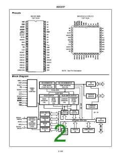
A0-A3
32-35
I/O
ADDRESS: The four least significant address lines are bidirectional three-state signals. In the Idle
cycle, they are inputs and are used by the 82C237 to address the control register to be loaded or
read. In the Active cycle, they are outputs and provide the lower 4-bits of the output address. When
in 16-bit mode (82C237 only), and the active channel is a 16-bit channel (as defined by the Data-
Width register), then A0 will remain low during the entire transfer (i.e. an even word address will al-
ways be generated).
A4-A7
HRQ
37-40
10
O
O
ADDRESS: The four most significant address lines are three-state outputs and provide 4-bits of
address. These lines are enabled only during the DMA service.
HOLD REQUEST: The Hold Request (HRQ) output is used to request control of the system bus.
When a DREQ occurs and the corresponding mask bit is clear, or a software DMA request is made,
the 82C237 issues HRQ. The HLDA signal then informs the controller when access to the system
busses is permitted. For stand-alone operation where the 82C237 always controls the busses, HRQ
may be tied to HLDA. This will result in one S0 state before the transfer.
DACK0-
DACK3
14, 15
24, 25
O
O
O
DMA ACKNOWLEDGE: DMA acknowledge is used to notify the individual peripherals when one
has been granted a DMA cycle. The sense of these lines is programmable. RESET initializes them
to active low.
AEN
9
8
ADDRESS ENABLE: Address Enable enables the 8-bit latch containing the upper 8 address bits
onto the system address bus. AEN can also be used to disable other system bus drivers during DMA
transfers. AEN is active HIGH.
ADSTB
ADDRESS STROBE: This is an active high signal used to control latching of the upper address
byte. It will drive directly the strobe input of external transparent octal latches, such as the 82C82.
During block operations, ADSTB will only be issued when the upper address byte must be updated,
thus speeding operation through elimination of S1 states. ADSTB timing is referenced to the falling
edge of the 82C237 clock.
MEMR
MEMW
DWLE
3
4
5
O
O
O
MEMORY READ: The Memory Read signal is an active low three-state output used to access data
from the selected memory location during a DMA Read or a memory-to-memory transfer.
MEMORY WRITE: The Memory Write is an active low three-state output used to write data to the
selected memory location during a DMA Write or a memory-to-memory transfer.
DATA-WIDTH, LATCH ENABLE: In normal 8-bit transfer mode (16-bit transfer mode not enabled),
this output is always high impedance three-stated. In 16-bit transfer mode (82C237 only), this output
serves a dual purpose. During S1 cycles, the DWLE output indicates the data width (0 = 16-bit, 1 =
8-bit) of the active channel. During memory-to-memory transfers, the DWLE output is used to enable
an external latch which temporarily stores the 8 most significant bits of data during the read-from-
memory transfer. DWLE enables this byte of data onto the data bus during the write-to-memory
transfer of a memory-to-memory operation.
4-151

 INTERSIL [ Intersil ]