82C237
Functional Description
The 82C237 is an improved version of the Intersil 82C37A been programmed into the controller via the Command,
DMA controller and is fully software and pin for pin compati- Mode, Address, and Word Count registers.
ble with the 82C37A. All operational and pin descriptions of
For example, if a block of data is to be transferred from RAM
the 82C37A apply to the 82C237 with additional features
to an I/O device, the starting address of the data is loaded
noted in the section titled 82C237 Operation.
into the 82C237 Current and Base Address registers for a
The 82C237 direct memory access controller is designed to particular channel, and the length of the block is loaded into
improve the data transfer rate in systems which must the channel’s Word Count register. The corresponding Mode
transfer data from an I/O device to memory, or move a block register is programmed for a memory-to-I/O operation (read
of memory to an I/O device. It will also perform memory-to- transfer), and various options are selected by the Command
memory block moves, or fill a block of memory with data register and the other Mode register bits. The channel’s
from a single location. Operating modes are provided to mask bit is cleared to enable recognition of a DMA request
handle single byte transfers as well as discontinuous data (DREQ). The DREQ can either be a hardware signal or a
streams, which allows the 82C237 to control data movement software command.
with software transparency.
Once initiated, the block DMA transfer will proceed as the
The DMA controller is a state-driven address and control controller outputs the data address, simultaneous MEMR
signal generator, which permits data to be transferred and IOW pulses, and selects an I/O device via the DMA
directly from an I/O device to memory or vice versa without acknowledge (DACK) outputs. The data byte flows directly
ever being stored in a temporary register. This can greatly from the RAM to the I/O device. After each byte is
increase the data transfer rate for sequential operations, transferred, the address is automatically incremented (or
compared with processor move or repeated string decremented) and the word count is decremented. The
instructions.
Memory-to-memory
operations
require operation is then repeated for the next byte. The controller
temporary internal storage of the data byte between stops transferring data when the Word Count register
generation of the source and destination addresses, so underflows, or an external EOP is applied.
memory-to-memory transfers take place at less than half the
rate of I/O operations, but still much faster than with central
processor techniques. The maximum data transfer rates
obtainable with the 82C237 are shown in Figure 1.
NAME
Base Address Registers
Base Word Count Registers
Current Address Registers
Current Word Count Registers
Temporary Address Register
Temporary Word Count Register
Status Register
SIZE
16-Bits
16-Bits
16-Bits
16-Bits
16-Bits
16-Bits
8-Bits
8-Bits
8-Bits
6-Bits
4-Bits
4-Bits
4-Bits
NUMBER
4
4
4
4
1
1
1
1
1
4
1
1
1
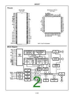
The block diagram of the 82C237 is shown on page 2. The
timing and control block, priority block, and internal registers
are the main components. Figure 2 lists the name and size
of the internal registers. The timing and control block derives
internal timing from CLK input, and generates external
control signals. The Priority Encoder block resolves priority
contention between DMA channels requesting service
simultaneously.
Command Register
82C237
TRANSFER
TYPE
8MHz
12.5MHz
Temporary Register
8-BIT 16-BIT 8-BIT 16-BIT
UNIT
Mode Registers
Compressed
Normal I/O
4.00
2.67
1.00
8.00
5.34
2.00
6.25
4.17
1.56
12.5
8.34
3.12
MByte/sec
MByte/sec
MByte/sec
Mask Register
Request Register
Memory-to-
Memory
Data-Width Register (See Note)
NOTE: 82C237 only
FIGURE 1. DMA TRANSFER RATES
FIGURE 2. 82C237 INTERNAL REGISTERS
DMA Operation
To further understand 82C237 operation, the states
generated by each CLK cycle must be considered. The DMA
controller operates in two major cycles, active and idle. After
being programmed, the controller is normally idle until a
DMA request occurs on an unmasked channel, or a software
request is given. The 82C237 will then request control of the
system busses and enter the active cycle. The active cycle is
composed of several internal states, depending on what
options have been selected and what type of operation has
been requested.
In a system, the 82C237 address and control outputs and
data bus pins are basically connected in parallel with the
system busses. An external latch is required for the upper
address byte. While inactive, the controller’s outputs are in a
high impedance state. When activated by a DMA request
and bus control is relinquished by the host, the 82C237
drives the busses and generates the control signals to
perform the data transfer. The operation performed by
activating one of the four DMA request inputs has previously
4-152

 INTERSIL [ Intersil ]