82C59A
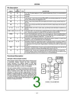
Priority Resolver
The Cascade Buffer/Comparator
This logic block determines the priorities of the bits set in the This function block stores and compares the IDs of all
lRR. The highest priority is selected and strobed into the cor- 82C59As used in the system. The associated three I/O pins
responding bit of the lSR during the INTA sequence.
(CAS0 - 2) are outputs when the 82C59A is used as a mas-
ter and are inputs when the 82C59A is used as a slave. As a
master, the 82C59A sends the ID of the interrupting slave
device onto the CAS0 - 2 lines. The slave, thus selected will
send its preprogrammed subroutine address onto the Data
Bus during the next one or two consecutive INTA pulses.
(See section “Cascading the 82C59A”.)
Interrupt Mask Register (IMR)
The lMR stores the bits which disable the interrupt lines to
be masked. The IMR operates on the output of the IRR.
Masking of a higher priority input will not affect the interrupt
request lines of lower priority.
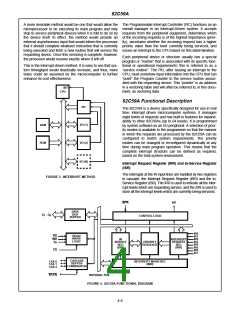
Interrupt Sequence
Interrupt (INT)
The powerful features of the 82C59A in a microcomputer
system are its programmability and the interrupt routine
addressing capability. The latter allows direct or indirect
jumping to the specified interrupt routine requested without
any polling of the interrupting devices. The normal sequence
of events during an interrupt depends on the type of CPU
being used.
This output goes directly to the CPU interrupt input. The
VOH level on this line is designed to be fully compatible with
the 8080, 8085, 8086/88, 80C86/88, 80286, and 80C286
input levels.
Interrupt Acknowledge (INTA)
INTA pulses will cause the 82C59A to release vectoring
information onto the data bus. The format of this data
depends on the system mode (µPM) of the 82C59A.
These events occur in an 8080/8085 system:
1. One or more of the INTERRUPT REQUEST lines
(IR0 - IR7) are raised high, setting the corresponding IRR
bit(s).
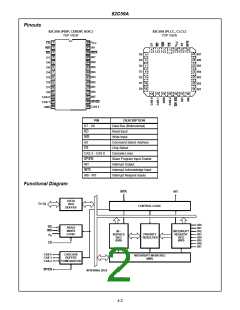
Data Bus Buffer
This 3-state, bidirectional 8-bit buffer is used to interface the
82C59A to the System Data Bus. Control words and status
information are transferred through the Data Bus Buffer.
2. The 82C59A evaluates those requests in the priority
resolver and sends an interrupt (INT) to the CPU, if
appropriate.
Read/Write Control Logic
3. The CPU acknowledges the lNT and responds with an
INTA pulse.
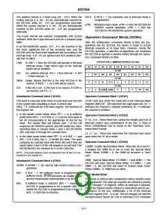
The function of this block is to accept output commands from
the CPU. It contains the Initialization Command Word (lCW)
registers and Operation Command Word (OCW) registers
which store the various control formats for device operation.
This function block also allows the status of the 82C59A to
be transferred onto the Data Bus.
4. Upon receiving an lNTA from the CPU group, the highest
priority lSR bit is set, and the corresponding lRR bit is
reset. The 82C59A will also release a CALL instruction
code (11001101) onto the 8-bit data bus through D0 - D7.
5. This CALL instruction will initiate two additional INTA
pulses to be sent to 82C59A from the CPU group.
Chip Select (CS)
A LOW on this input enables the 82C59A. No reading or 6. These two INTA pulses allow the 82C59A to release its
writing of the device will occur unless the device is selected.
preprogrammed subroutine address onto the data bus.
The lower 8-bit address is released at the first INTA pulse
and the higher 8-bit address is released at the second
INTA pulse.
Write (WR)
A LOW on this input enables the CPU to write control words
(lCWs and OCWs) to the 82C59A.
7. This completes the 3-byte CALL instruction released by
the 82C59A. In the AEOI mode, the lSR bit is reset at the
end of the third INTA pulse. Otherwise, the lSR bit
remains set until an appropriate EOI command is issued
at the end of the interrupt sequence.
Read (RD)
A LOW on this input enables the 82C59A to send the status
of the Interrupt Request Register (lRR), In-Service Register
(lSR), the Interrupt Mask Register (lMR), or the interrupt
level (in the poll mode) onto the Data Bus.
The events occurring in an 80C86/88/286 system are the
same until step 4.
A0
4. The 82C59A does not drive the data bus during the first
INTA pulse.
This input signal is used in conjunction with WR and RD sig-
nals to write commands into the various command registers,
as well as to read the various status registers of the chip.
This line can be tied directly to one of the system address
lines.
5. The 80C86/88/286 CPU will initiate a second INTA pulse.
During this INTA pulse, the appropriate ISR bit is set and
the corresponding bit in the IRR is reset. The 82C59A
outputs the 8-bit pointer onto the data bus to be read by
the CPU.
4-5

 INTERSIL [ Intersil ]