82C59A
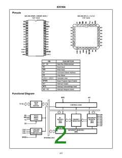
Pin Description
PIN
SYMBOL
NUMBER
TYPE
DESCRIPTION
: The +5V power supply pin. A 0.1µF capacitor between pins 28 and 14 is recommended for
V
28
I
V
CC
CC
decoupling.
GND
CS
14
1
I
I
GROUND
CHIP SELECT: A low on this pin enables RD and WR communications between the CPU and the
82C59A. INTA functions are independent of CS.
WR
RD
2
3
I
WRITE: A low on this pin when CS is low enables the 82C59A to accept command words from
the CPU.
I
READ: A low on this pin when CS is low enables the 82C59A to release status onto the data bus
for the CPU.
D7 - D0
4 - 11
I/O
I/O
I/O
BIDIRECTIONAL DATA BUS: Control, status, and interrupt-vector information is transferred via
this bus.
CAS0 - CAS2 12, 13, 15
CASCADE LINES: The CAS lines form a private 82C59A bus to control a multiple 82C59A struc-
ture. These pins are outputs for a master 82C59A and inputs for a slave 82C59A.
SP/EN
16
SLAVE PROGRAM/ENABLE BUFFER: This is a dual function pin. When in the Buffered Mode it
can be used as an output to control buffer transceivers (EN). When not in the Buffered Mode it is
used as an input to designate a master (SP = 1) or slave (SP = 0).
INT
17
O
I
INTERRUPT: This pin goes high whenever a valid interrupt request is asserted. It is used to inter-
rupt the CPU, thus, it is connected to the CPU's interrupt pin.
IR0 - IR7
18 - 25
INTERRUPT REQUESTS: Asynchronous inputs. An interrupt request is executed by raising an
IR input (low to high), and holding it high until it is acknowledged (Edge Triggered Mode), or just
by a high level on an IR input (Level Triggered Mode). Internal pull-up resistors are implemented
on IR0 - 7.
INTA
A0
26
27
I
I
INTERRUPT ACKNOWLEDGE: This pin is used to enable 82C59A interrupt-vector data onto the
data bus by a sequence of interrupt acknowledge pulses issued by the CPU.
ADDRESS LINE: This pin acts in conjunction with the CS, WR, and RD pins. It is used by the
82C59A to decipher various Command Words the CPU writes and status the CPU wishes to read.
It is typically connected to the CPU A0 address line (A1 for 80C86/88/286).
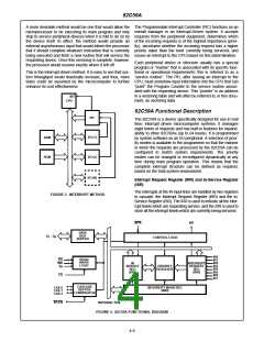
Functional Description
CPU - DRIVEN
MULTIPLEXER
Interrupts in Microcomputer Systems
CPU
Microcomputer system design requires that I/O devices such
as keyboards, displays, sensors and other components
receive servicing in an efficient manner so that large
amounts of the total system tasks can be assumed by the
microcomputer with little or no effect on throughput.
RAM
ROM
I/O (1)
I/O (2)
The most common method of servicing such devices is the
Polled approach. This is where the processor must test each
device in sequence and in effect “ask” each one if it needs
servicing. It is easy to see that a large portion of the main
program is looping through this continuous polling cycle and
that such a method would have a serious, detrimental effect
on system throughput, thus, limiting the tasks that could be
assumed by the microcomputer and reducing the cost effec-
tiveness of using such devices.
I/O (N)
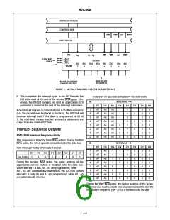
FIGURE 2. POLLED METHOD
4-3

 INTERSIL [ Intersil ]