28F020
E
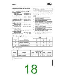
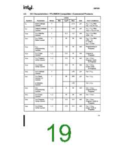
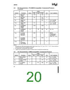
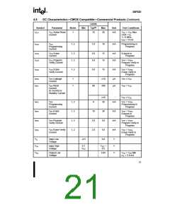
4.0 ELECTRICAL SPECIFICATIONS
NOTICE: This is a production datasheet. The specifications
are subject to change without notice.
*WARNING: Stressing the device beyond the Absolute
Maximum Ratings may cause permanent damage. These
are stress ratings only. Operation beyond the Operating
Conditions is not recommended and extended exposure
beyond the Operating Conditions may affect device
reliability.
4.1
Absolute Maximum Ratings*
Operating Temperature
During Read .........................0 °C to +70 °C(1)
During Erase/Program..........0 °C to +70 °C(1)
Operating Temperature
NOTES:
During Read .....................–40 °C to +85 °C(2)
During Erase/Program......–40 °C to +85 °C(2)
1. Operating temperature is for commercial product
defined by this specification.
Temperature Under Bias.........–10 °C to +80 °C(1)
Temperature Under Bias.........–50 °C to +95 °C(2)
Storage Temperature...............–65 °C to +125 °C
2. Operating temperature is for extended temperature
product as defined by this specification.
3. Minimum DC input voltage is –0.5 V. During transitions,
inputs may undershoot to –2.0 V for periods less than
20 ns. Maximum DC voltage on output pins is VCC
0.5 V, which may overshoot to VCC + 2.0 V for periods
less than 20 ns.
+
Voltage on Any Pin with
Respect to Ground ............–2.0 V to +7.0 V(2)
Voltage on Pin A9 with
4. Maximum DC voltage on A9 or VPP may overshoot to
+14.0 V for periods less than 20 ns.
Respect to Ground ........–2.0 V to +13.5 V(2,3)
5. Output shorted for no more than one second. No more
than one output shorted at a time.
VPP Supply Voltage with
Respect to Ground
During Erase/Program...–2.0 V to +14.0 V(2,3)
6. See Testing Input/Output Waveform (Figure 6) and AC
Testing Load Circuit (Figure 7) for testing
characteristics.
VCC Supply Voltage with
7. See High Speed AC Testing Input/Output Waveform
(Figure 8) and High Speed AC Testing Load Circuit
(Figure 9) for testing characteristics.
Respect to Ground ............–2.0 V to +7.0 V(2)
Output Short Circuit Current.................. 100 mA(4)
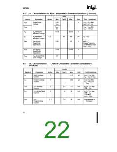
4.2
Operating Conditions
Limits
Symbol
Parameter
Min
0
Max
70
Unit
°C
°C
V
TA
TA
Operating Temperature(1)
Operating Temperature(2)
VCC Supply Voltage (10%)(6)
VCC Supply Voltage (5%)(7)
–40
4.50
4.75
+85
5.50
5.25
VCC
VCC
V
4.3
Capacitance
TA = 25 °C, f = 1.0 MHz
Limits
Min
Symbol
Parameter
Notes
Max
8
Unit
Conditions
VIN = 0 V
CIN
Address/Control Capacitance
Output Capacitance
1
1
pF
pF
COUT
12
VOUT = 0 V
NOTE:
1. Sampled, not 100% tested.
18

 INTEL [ INTEL ]