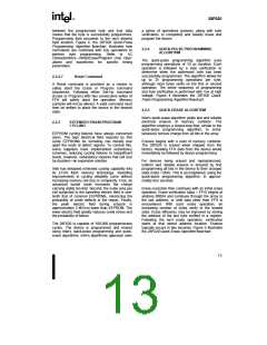
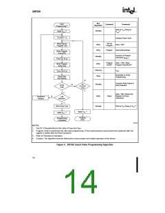
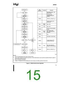
28F020
E
Bus
Operation
Start
Command
Comments
Programming (4)
Wait for VPP Ramp to
(1)
Standby
Apply VPPH
(1)
VPPH
PLSCNT = 0
Initialize Pulse-Count
Set-Up
Program
Write Set-Up
Program Cmd
Write
Write
Data = 40H
Program
Valid Address/Data
Duration of Program
Write Program
Cmd (A/D)
Standby
Write
Operation (tWHWH1
)
Time Out 10 µs
Program
Verify(2)
Data = C0H; Stops
(3)
Write Program
Verify Cmd
Program Operations
Stand-by
Read
tWHGL
Time Out 6 µs
Read Byte to Verify
Programming
Read Data
from Device
N
Compare Data Output to
Data Expected
Inc
PLSCNT
=25?
Standby
N
Verify
Data
Y
Y
Data = 00H, Resets the
Register for Read
Operations
Write
Read
N
Increment
Address
Last
Address?
Y
(1)
Write Read Cmd
Standby
Wait for VPP Ramp to VPPL
(1)
Apply VPPL
(1)
Apply VPPL
Program
Error
Programming
Completed
0245_04
NOTES:
1. See DC Characteristics for the value of VPPH and VPPL
.
2. Program Verify is performed only after byte programming. A final read/compare may be performed (optional) after the
register is written with the Read command.
3. Refer of Principles of Operation.
4. Caution: The algorithm must be followed to ensure proper and reliable operation of the device.
Figure 4. 28F020 Quick-Pulse Programming Algorithm
14

 INTEL [ INTEL ]